Development of GaN-Based UV LEDs: Challenges and Emerging Solutions
published: 17 July 2025 | https://doi.org/10.63174/xdi.ADXX2196
Abstract
Gallium nitride (GaN) and its related alloys, particularly aluminum gallium nitride (AlGaN), have emerged as promising materials for deep ultraviolet light-emitting diodes (DUV LEDs) due to their wide bandgap properties and solid-state emission advantages. These devices show broad application potential in areas such as water purification, biological sterilization, and medical diagnostics. However, DUV LEDs currently face significant challenges in terms of external quantum efficiency (EQE), thermal management, and device reliability. This review systematically summarizes the key limitations that hinder the performance of AlGaN-based DUV LEDs, including difficulties in achieving efficient p-type doping in high-Al-content materials, poor carrier injection efficiency, high thermal resistance, and high defect densities. In response to these bottlenecks, various state-of-the-art strategies aimed at improving both internal and external quantum efficiency are discussed, such as quantum well structure optimization, polarization-engineered tunnel junctions, crystalline quality enhancement, interface band engineering, and advanced light extraction designs. Furthermore, the review highlights critical approaches for reducing thermal resistance and enhancing device reliability, including the use of high thermal conductivity substrates, advanced packaging technologies, and thermal interface materials. Overall, the advancement of AlGaN-based DUV LEDs relies on coordinated innovations in materials, device architecture, and system-level integration to realize high-efficiency, high-reliability performance.
1. Introduction
GaN and its derived alloys, such as AlGaN, have emerged as promising materials for ultraviolet (UV) light-emitting diodes (LEDs) due to their wide bandgap and solid-state cooling characteristics, offering significant application potential in water disinfection, air purification, biomedical treatment, and sterilization fields[1,2]. Environment-friendly AlGaN-based UVB LEDs with monochromatic light emission are inevitable for both medical and agricultural applications[3-7]. The selection of green AlGaN material has many other promising features, such as high internal-quantum-efficiency (IQE) from the multi-quantum-well (MQWs) as well as reasonable level of optical and electrical properties[8]. The AlGaN-based semiconductors assist in substantial reduction of UV LED and LD production cost, partially due to their ability to be monolithically grown on low-cost c-sapphire substrates in low-pressure metal–organic vapour phase epitaxy (LP-MOVPE) reactors[9]. Compared to conventional mercury-based UV lamps, which are toxic and environmentally hazardous, AlGaN-based UV LEDs offer advantages such as energy efficiency, environmental friendliness, compact size, and rapid response[1,10]. For instance, the COVID-19 pandemic has spurred intensive research into disinfection-grade UV LEDs operating in the 220–240 nm wavelength range; however, the efficiency and reliability of these deep UV emitters still fall short of practical requirements[1,10]. AlGaN alloy is determined to have a tunable direct bandgap (3.4–6.11 eV). This is found to be suitable material for the manufacturing of optical devices[11-14].Although substantial progress has been made in the development of AlGaN-based UV LEDs in recent years [15,16], their performance remains significantly inferior to that of visible InGaN-based LEDs. GaN-based UV emitters face numerous challenges, including low p-type doping efficiency in AlGaN materials, inefficient carrier injection, poor thermal management, and a high density of structural defects[17]. This review provides an in-depth analysis of these critical issues and explores potential solutions from the perspectives of enhancing both IQE and light extraction efficiency (LEE). Key strategies discussed include quantum well design, tunnel injection structures, crystal quality improvement, interface engineering, and optimization of light extraction architectures[18]. In addition, we examine technological approaches for reducing thermal resistance and improving device reliability, such as material modification, thermal interface materials, thermal management structures, and advanced packaging techniques, aiming to provide a comprehensive reference for the development of high-performance GaN-based UV LEDs.
2. Key Challenges in the Fabrication of AlGaN Materials
With the continuous advancement of deep ultraviolet (DUV) optoelectronic technologies, AlGaN-based LEDs have become indispensable due to their tunable bandgap and superior thermal stability. Nonetheless, high-Al-content AlGaN materials still encounter substantial challenges in p-type doping, carrier injection, thermal management, and epitaxial quality, which critically constrain device quantum efficiency and reliability. A thorough examination of these fabrication bottlenecks and the corresponding mitigation strategies is therefore essential for the further development of high-performance DUV LEDs. This review systematically addresses these key issues and highlights recent research progress.
2.1. Low p-Type Doping Efficiency
P-type doping in AlGaN alloys, particularly at high Al compositions, exhibits very low efficiency, with Mg as the main dopant[10,19]. This is mainly due to: (1) limited Mg solubility caused by high formation enthalpy; (2) increasing Mg acceptor activation energy from ~170 meV in GaN to ~630 meV in AlN, which impedes hole ionization; (3) strong self-compensation by donor-like native defects (e.g., nitrogen vacancies) forming charge-neutral complexes with Mg, reducing free hole generation[10,19]. Consequently, p-type doping efficiency in high-Al-content AlGaN remains below 1%[10,19]. Although methods like laser activation and multi-step Mg doping have increased hole concentrations above 10¹⁷ cm⁻³ for AlGaN with ~70% Al[20], these levels are still insufficient for efficient hole injection in DUV LEDs.
To address the low p-type doping efficiency, several optimization strategies have been developed. Methods including Mg-δ doping[21], modulation doping in MQWs[22], and Mg–Si co-doping[23] effectively reduce Mg activation energy and enhance hole concentration[24-27]. Additionally, polarization-induced doping leverages built-in electric fields in AlGaN superlattices or composition-graded layers to significantly increase hole density[10,15], while polarization-matched quantum wells, which are designed to balance polarization fields across interfaces, help minimize band bending and enhance carrier confinement. For example, embedding periodically graded superlattice (SL), which consist of periodic multilayer structures such as alternating AlGaN layers and enable strain relaxation, defect reduction, and band engineering to enhance doping efficiency and carrier transport, within AlGaN layers can generate interfacial charge accumulation. Producing built-in electric fields that assist hole ionization and significantly improve the conductivity of the p-type layer[10,23]. Surface treatment and interface engineering—such as indium surfactants and superlattice interlayers—have been utilized to enhance Mg solubility and doping uniformity[28]. These approaches demonstrate that optimized growth and material design can significantly improve p-type doping efficiency in AlGaN. However, achieving doping performance on par with GaN remains a significant challenge.
2.2. Challenges in Carrier Injection
Low carrier injection efficiency in ultraviolet LEDs stems primarily from inefficient p-type doping[10]. Furthermore, device-level carrier transport barriers worsen injection performance, including low hole concentration in high-Al-content AlGaN, severe electron leakage due to weak electron blocking layer (p-EBL) which is inserted between the active region and the p-side to suppress electron leakage and employed for electron confinement but may also hinder hole injection due to the energy barriers it introduces, confinement, and reduced radiative recombination caused by the quantum-confined Stark effect in multiple quantum wells[29-32]. In conventional PIN structures, the p-EBL is used for electron confinement; however, it simultaneously introduces significant resistance to hole transmission[10]. Consequently, electron overflow into the p-region and limited hole injection into the active region severely reduce radiative recombination efficiency[10,33]. Simulations reveal that AlGaN UV LEDs commonly exhibit “electron overflow and hole deficiency,” causing a pronounced drop in IQE at high injection currents[10,33].
To enhance carrier injection efficiency, various engineering strategies have been proposed. Notably, tunnel junctions (TJs), which are highly doped p–n junctions that allow carriers to quantum-tunnel through the depletion region, enabling efficient injection even in materials with poor conductivity, replace the conventional p-GaN layer with an n-GaN/Mg-doped p-type structure, leveraging tunneling under reverse bias to inject holes into MQWs[28]. Zhang et al. demonstrated that polarization-engineered AlGaN tunnel junctions can reduce tunnel resistance below 2 mΩ·cm² even for high-Al-content materials (up to AlN), enhancing EQE to 3.4% in UV-A/UV-B LEDs[28]. Secondly, optimization of EBLs—including graded Al composition, composite, and superlattice structures—utilizes polarization charges to improve band alignment, increasing electron barrier height while lowering hole injection barriers. For example, linearly increasing Al content along the p-EBL induces polarization fields that facilitate hole injection[10,34]. Thirdly, hole injection layers (HILs), such as thin GaN layers or superlattices between p-AlGaN and GaN, serve as low-energy hole sources, enhancing hole supply[2,33]. Yang et al. reported that a p-AlGaN/p-GaN thin-well superlattice HIL increased hole concentration by an order of magnitude, effectively mitigating IQE droop at high currents[34]. Additionally, introducing polarization fields in EBL or p-type layers (e.g., negatively charged anion-polarization layers) and exploring nonpolar or semipolar crystal orientations have been proposed to reduce polarization-induced carrier injection barriers and improve hole injection efficiency[35,36].
2.3. Thermal Management Challenges
DUV LEDs operate at high current densities, generating significant heat. However, the low thermal conductivity of AlGaN and conventional substrates like sapphire leads to elevated junction temperatures and rapid performance degradation[37]. Thermal expansion and lattice mismatches in heterogeneous epitaxy further reduce IQE[38-40]. For example, sapphire’s thermal conductivity (~35 W/m·K) is much lower than intrinsic GaN or AlN, hindering heat dissipation. Transferring LED chips from sapphire to high-thermal-conductivity substrates such as AlN, SiC, or diamond via flip-chip bonding significantly lowers thermal resistance and improves heat dissipation[37]. Composite diamond-AlN substrates combine high thermal conductivity with better lattice matching[41]. Liu et al. reported that AlN substrates bonded with metal agents reduced packaging thermal resistance to ~4.6 K/W, enhancing output power[42]. Burkhardt et al. demonstrated multi-chip UV LED packages using AlN ceramics and copper alloy substrates with thermal conductivity up to 180 W/m·K, greatly improving thermal management. Zhang et al. applied 3D-printed micro-jet cooling to further enhance GaN device heat dissipation[43].
High-thermal-conductivity die-attach materials (e.g., silver nanopaste, silver sintering pastes), flip-chip packaging, and multilayer heat sinks are commonly employed to enhance heat conduction[44]. Direct contact with polished or metal heat sinks further improves heat dissipation, preventing overheating and performance degradation. Elevated temperatures during packaging can impair chip performance and accelerate material aging, reducing reliability. Thus, effective thermal management is essential to maintain device reliability, optical output, luminous efficiency, and lifespan[45-47]. Traditional EMC packaging exhibits thermal resistance ranging from 32 K/W (low-power LEDs) to 9.9 K/W (high-power LEDs), mainly due to low vertical thermal conductivity and high interface resistance[48,49]. Overall, DUV LED thermal management requires an integrated strategy encompassing material choice, chip design, and packaging to minimize thermal resistance and ensure long-term reliability[37,44].
2.4 Other Challenges
High-Al-content AlGaN epitaxial layers often exhibit significant internal stress, causing cracking and pinhole defects. AlGaN grown on GaN templates experiences in-plane tensile stress, making it prone to cracking[50]. Use of AlN substrates or nano-patterned templates has been proposed to partially relax this stress. The narrow growth window of high-Al-content AlGaN poses additional challenges: increasing ammonia flow or lowering pressure to enhance AlN nucleation can introduce defects, while higher growth rates may cause undesirable gas-phase reactions. Halide vapor phase epitaxy (HVPE) with chloride precursors offers a promising alternative for rapid growth of high-quality thick AlGaN layers across wide compositions. Optimized HVPE processes demonstrated by the SCIOCS team in Japan may enable relaxed, free-standing AlGaN substrates, reducing series resistance and self-heating.
Material quality degradation critically limits DUV LED efficiency. Severe lattice mismatch with sapphire substrates induces high-density threading dislocations (~10⁹–10¹⁰ cm⁻²), which act as non-radiative recombination and scattering centers[51]. Screw dislocations can extend through the LED structure, forming defect clusters that serve as parasitic recombination sites and dopant compensators, degrading IQE[51].
Interface issues further limit performance. The conventional p-GaN contact layer strongly absorbs DUV photons, reducing LEE[52]. Atomic layer deposition (ALD) passivation layers effectively suppress non-radiative centers[53]. Additionally, interface roughness, interlayer stress, and polarization-induced charges distort internal electric fields in AlGaN multilayers, trapping carriers and lowering radiative recombination efficiency. Collectively, these material and interface challenges substantially constrain AlGaN-based UV LED performance.
3. Strategies for Enhancing Internal and External Quantum Efficiency
IQE and external quantum efficiency (EQE) remains a core challenge in DUV LED development. IQE is mainly constrained by carrier recombination efficiency and crystal defects, while EQE is additionally influenced by LEE and carrier injection. Inherent difficulties in lattice matching, doping, and optical design of AlGaN materials result in DUV LED efficiencies far below those of visible LEDs. Recent advances encompass quantum well optimization, tunnel junction integration, enhanced epitaxial quality, polarization field modulation through interface engineering, and optical design improvements to increase LEE. Emerging approaches such as nonpolar/semipolar growth, micro-LED arrays, and novel transparent electrodes present promising routes to surpass current efficiency barriers.
3.1. Quantum Well Optimization
The QW structure serves as the active region of light emission in LEDs, and its design plays a critical role in determining the carrier recombination efficiency. For AlGaN-based MQWs, optimization strategies include tailoring the well/barrier configuration, implementing strain engineering, and modulating impurity doping and distribution. For instance, reducing the quantum well width can mitigate the quantum-confined Stark effect (QCSE), which refers to the spatial separation of electrons and holes in quantum wells caused by strong internal electric fields, thereby enhancing the electron–hole overlap. Introducing Mg-δ doping or superlattices in the barrier layers can generate internal electric fields that facilitate hole capture[10,19]. Recent studies have demonstrated that co-doping with silicon in the barriers can induce space charge regions, further improving recombination efficiency[54]. Moreover, the incorporation of InAlN or AlGaN multilayers within QWs to form composite well structures has been shown to enhance carrier injection while suppressing electron overflow. Wu et al. employed trapezoidal QWs to boost the output power of green LEDs[55], offering insights for QW shape design. Zhanghu et al. revealed a strong correlation between IQE and the ideality factor in InGaN micro-LEDs, providing valuable guidance for QW modulation[56]. Tsai et al. investigated the competing mechanisms of Auger recombination and carrier leakage in MQWs, which is essential for improving emission efficiency[57]. Strain engineering is another effective strategy: applying external strain or designing strain gradients can modulate the valence band edge to favor transverse electric (TE) polarization emission, thereby enhancing light output[16,58]. Wang et al. reported that inserting alternating AlN/AlGaN superlattice layers significantly reduced crystal defects and strain mismatch in AlN layers, increasing the relative IQE of 280 nm MQWs from 22.8% to 85%[16]. Figure 1 illustrates the device performance enhancement achieved by Wang et al. through the integration of AlN/AlGaN superlattices into AlGaN MQWs.
Figure 1. (a) Shows that the sample with the introduced superlattice structure exhibits a higher photoluminescence (PL) intensity; (b) indicates that its relative IQE increases from 22.8% to 85%[16].
Additionally, three-dimensional confinement structures, such as quantum dots (QDs) and quantum rods, can effectively suppress carrier diffusion into defect-rich regions. GaN/AlN self-assembled quantum dots provide strong lateral and vertical carrier confinement, which helps inhibit non-radiative recombination. Experimental results have shown that GaN/AlN quantum dot LEDs exhibit significantly higher IQE compared to AlGaN quantum wells emitting at similar wavelengths. For example, one report demonstrated that a 300 nm GaN quantum dot LED achieved a room-temperature IQE of approximately 62%[58], far exceeding that of planar quantum well structures in the same spectral range. This enhancement is mainly attributed to the strong carrier confinement in quantum dots and their reduced sensitivity to defects[59]. Although the growth of quantum dots presents technical challenges, their inherent advantages in reducing non-radiative losses make them a promising approach for improving IQE.
3.2. Tunnel Injection Structures
Tunnel junction structures transform the carrier injection mechanism from the conventional p–i–n approach to an “n–p” tunneling injection, fundamentally overcoming the limitations of poor p-type conductivity and significantly improving hole injection efficiency[60,61]. Furthermore, reverse-polarized AlN/InGaN tunnel junctions have been utilized to achieve low-resistance and highly efficient tunneling hole injection[62,63].Figure 2 compares the core structural differences between traditional ultraviolet LEDs and tunnel junction ultraviolet LEDs. The conventional structure relies on the p-type layer for hole injection (left), whereas the tunnel junction structure (right) employs an n-type contact layer combined with polarization-engineered heterojunctions (such as AlGaN/InGaN) to realize reverse tunneling hole injection while avoiding optical absorption. The energy band diagram illustrates that the strong electric field induced by polarization significantly bends the band edges, reducing the tunneling barrier from the wide-bandgap AlGaN (~5 eV) to the narrow-bandgap InGaN (~2 eV), thereby overcoming the p-type conductivity limitations. By inserting a tunnel junction layer (e.g., heavily doped GaN/AlGaN layers) between p-GaN and n-AlGaN, reverse tunneling injection is achieved under an applied electric field[64].
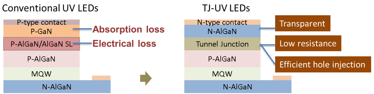
Figure 2. Schematic comparison between conventional UV LED structures and the tunnel junction-based UV LED structure[28].
Zhang et al. utilized polarization engineering to design a tunnel junction at the AlGaN heterojunction, creating a strong polarization field that significantly reduces the tunneling barrier[28]. Figure 3 demonstrates the successful experimental realization of an AlGaN tunnel junction with an Al composition as high as 75%, achieving a tunnel junction resistance below 2 mΩ·cm² and an EQE of 3.37% in the UV-A range[28]. Similarly, Yoo et al. have verified that a thinner GaN tunnel layer can effectively inject holes while maintaining low resistance. Additionally, studies have combined tunnel junctions with backside emission designs, simultaneously enhancing injection efficiency and optimizing light extraction[64]. These structures are predominantly grown by molecular beam epitaxy (MBE) or metal-organic chemical vapor deposition (MOCVD), showing great potential for improving the efficiency of deep ultraviolet LEDs[28].
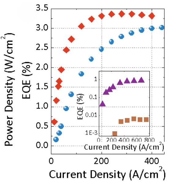
Figure 3. The optoelectronic performance of deep ultraviolet LEDs as a function of current density is shown in. The main graph depicts the variation of power density (blue circles) and EQE, red diamonds over a current density range of 0.01 to 800 A/cm². The EQE reaches a peak value of 3.37% at 200 A/cm², while the power density increases linearly up to 3.0 W/cm². The inset zooms in on the low current region (0.001–1 A/cm²), showing EQE (purple triangles) and power conversion efficiency (brown squares), revealing efficient hole injection characteristics of the tunnel junction structure under microcurrent conditions (logarithmic scale)[28].
Additionally, Cardozo et al. employed magneto-electroluminescence spectroscopy to investigate carrier density and dynamics in tunnel diodes, providing an effective tool for in-depth analysis of carrier injection mechanisms in ultraviolet LEDs[65]. Deng et al. experimentally demonstrated the feasibility and high injection efficiency of fully AlGaN-based tunnel junction structures in deep ultraviolet LEDs[66]. Furthermore, Sang et al. successfully applied tunnel junction structures to GaN-based micro-LEDs, significantly enhancing current injection capability[67]. Kim et al. further developed InGaN tunnel junction nanostructures in micro-lasers, exhibiting excellent carrier control and structural tunability[68].
3.3. Improvement of Crystal Quality
The presence of crystal defects, especially dislocations, introduces numerous non-radiative recombination centers, severely reducing the IQE. Therefore, improving the epitaxial quality of AlGaN heterostructures is fundamental to enhancing IQE. Figure 4 illustrates the design of a superlattice p-EBL structure[69]. The conventional p-EBL is typically a single high-Al-content AlGaN layer, which hinders hole injection. By replacing it with an alternately arranged AlGaN superlattice (e.g., Al₀.₆Ga₀.₄N/Al₀.₈Ga₀.₂N), the hole transport barrier height is significantly reduced while maintaining strong electron blocking capability. Experimental results show that this structure increases the hole concentration to nearly 10¹⁸ cm⁻³ and achieves nearly droop-free deep ultraviolet LED performance, validating its dual advantages of optimized carrier injection and suppressed electron leakage.
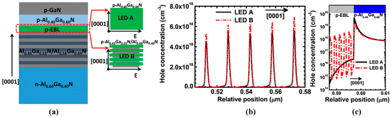
Figure 4. (a) Schematic structures for DUV LEDs with p-Al0.60Ga0.40N EBL (LED A) and p-Al0.60Ga0.40N/p-Al0.45Ga0.55N superlattice EBL (LED B). Numerically calculated hole concentration profiles (b) in the MQWs, (c) in the p-EBLs and p-Al0.40Ga0.60N layers for LEDs A and B[38].
Figure 5 illustrates the introduction of a superlattice electron deceleration layer (SEDL), where a stepped Al composition superlattice (e.g., from Al₀.₇Ga₀.₃N to Al₀.₅Ga₀.₅N) is incorporated into the n-type AlGaN layer. This design leverages polarization-induced electric fields to reduce the electron kinetic energy ("cooling" the electrons), thereby enhancing the probability of electron capture by the quantum wells[70]. Both experimental results and numerical simulations demonstrate that the SEDL structure increases the radiative recombination efficiency by approximately 30%, significantly improving the IQE and EQE. This approach effectively addresses the electron leakage issue caused by traditional high-Al-content barriers and offers a novel strategy for optimizing carrier dynamics in deep ultraviolet LEDs.
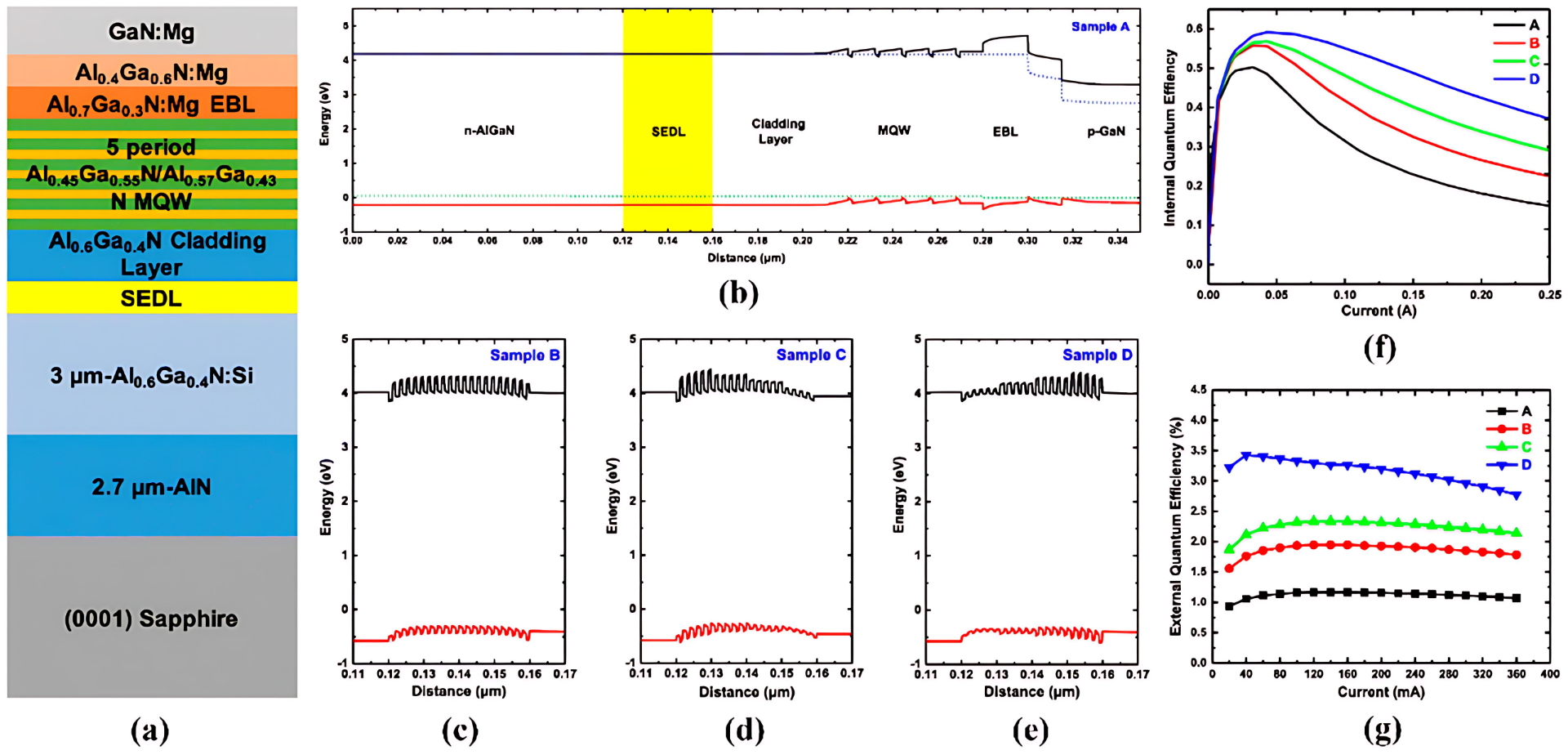
Figure 5. (a) Schematic of DUV LEDs. (b) Schematic band diagram of conventional DUV LEDs. (c–e) Three different super lattice electron deceleration layers. (f) IQE and (g) EQE as functions of current for the four DUV LEDs[70].
Meanwhile, the use of high-quality substrates and buffer layers is also a crucial approach. Guerin et al. systematically investigated the influence of basal plane stacking faults in AlN nanowires on their optical properties[71]. Bruckbauer et al. demonstrated that micropatterning of growth templates can significantly reduce defect densities in nonpolar GaN[72]. Additionally, Tatebayashi et al. revealed the formation mechanism and photoluminescence characteristics of GaN:Eu nanowires, providing new insights for the optimized design of doped luminescent materials[73]. Moreover, intrinsic AlN substrates offer ultra-low dislocation densities, which substantially enhance the performance of ultraviolet LEDs. As early as 2004, reports showed that DUV LEDs epitaxially grown on high-quality AlN substrates exhibited a saturation injection current twice that of samples grown on sapphire substrates[74]. Recently, Yoshikawa et al. employed high-quality AlN substrates for 233 nm LEDs, achieving an EQE of 0.25%[74], markedly outperforming sapphire-based devices. In addition to AlN substrates, GaN-based nano-templates have been explored to alleviate thermal stress and induce selective growth, thereby improving epitaxial quality[75]. For example, silicon substrates, which are low-cost and possess good thermal conductivity, have also been used[74], although they face challenges related to lattice mismatch during epitaxy. In practical applications, substrate selection and matched buffer layer design are tailored to minimize thermal expansion coefficient differences and reduce stress concentration.
Figure 6(a) shows that on AlN substrates (black squares), the silicon doping concentration exhibits an almost ideal linear relationship with the carrier concentration (e.g., when Si = 5 × 10¹⁹ cm⁻³, the carrier concentration reaches 4 × 10¹⁹ cm⁻³). In contrast, sapphire substrates (red/blue dots) suffer from severe impurity compensation due to high defect densities, resulting in carrier concentrations that are only 1/10 to 1/100 of those on AlN substrates. This demonstrates that AlN substrates can significantly enhance doping efficiency. Figure 6(b) compares the temperature-dependent conductivity, where epitaxial AlN:Si (blue squares) shows the highest conductivity (0.1 Ω⁻¹·cm⁻¹) at high temperature (900 K). Ion-implanted samples annealed at 1500 °C on AlN substrates (red squares) exhibit conductivity close to that of the epitaxial samples, while sapphire substrate samples (black triangles) show conductivity one order of magnitude lower (0.003 Ω⁻¹·cm⁻¹). These results indicate that AlN substrates, through their low defect density and high thermal conductivity, ensure high-temperature stability and mitigate ion implantation damage, providing a solid material foundation for high-efficiency deep ultraviolet devices[76].
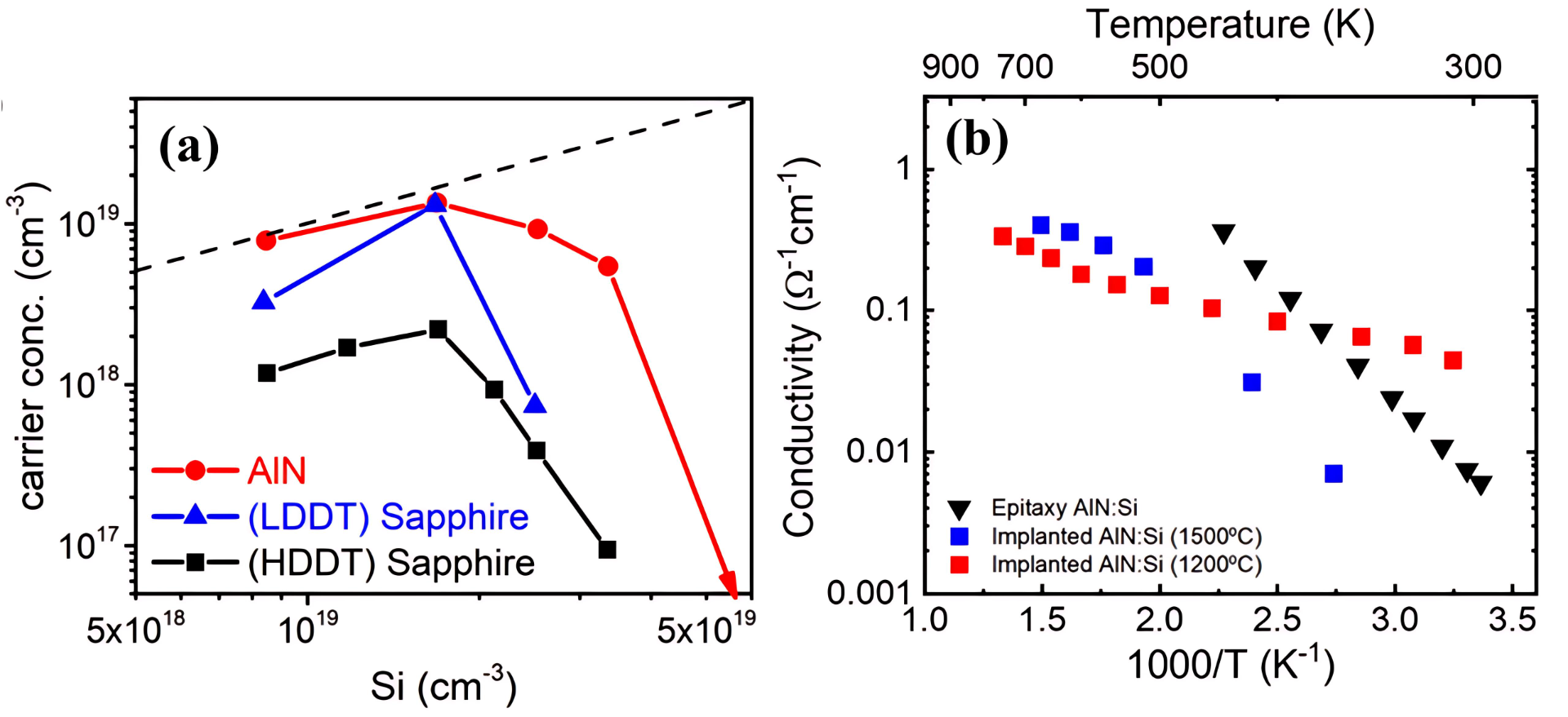
Figure 6. (a) The conductivity of n-AlGaN on different substrate with increasing Si doping concentration. (b) Temperature dependent conductivity for the epitaxially doped AlN film, the Si-implanted AlN film on sapphire, and the Si-implanted AlN film on AlN substrate[76,77].
3.4. Interface Engineering
Interface engineering primarily involves tailoring the polarization fields and carrier barriers at heterojunctions or quantum well interfaces through material design. For example, introducing a polarity charge layer at the interface between the p-EBL and p-AlGaN can neutralize the depletion field at the interface and reduce the hole injection barrier. One study demonstrated that incorporating an AlGaN compositional grading layer within the p-layer effectively reduced polarization mismatch at the top of the p-EBL, significantly enhancing hole transport efficiency[2,10]. Additionally, localized tuning of the polarization field by controlling the distribution of In atoms in AlGaN can maximize the overlap of carrier wavefunctions, thus improving recombination efficiency[78,79].Similarly, inserting a thin AlGaN layer beneath the p-GaN layer—referred to as a “polarization charge reservoir”—can attract electrons and release holes, thereby enhancing hole supply[10,33]. Figure 7(a) and 7(b) compare the conventional and improved p-AlGaN EBL structures: the improved design introduces an AlGaN compositional grading layer (L1/L2) within the EBL, which forms a polarization charge reservoir that neutralizes interface polarization fields, lowers the hole injection barrier, and suppresses electron leakage. Performance curves in Figure 7(c) and 7(d) show that the improved device B exhibits significantly higher optical power (~15 mW) and external quantum efficiency (~5%) at 250 mA compared to the conventional device A (~9 mW and 3%), and its efficiency droop at high current is notably mitigated. Experimental and simulation results consistently confirm that the graded EBL optimizes carrier transport, thereby enhancing the light output and efficiency stability of ultraviolet LEDs.
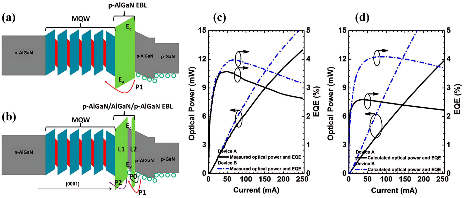
Figure 7. Schematic energy band diagrams for (a) DUV LEDs with the conventional p-AlGaN EBL and (b) DUV LEDs with the p-AlGaN/AlGaN/p-AlGaN EBL. (c) Experimentally tested and (d) numerically computed EQE and optical power at different injection current levels for devices A and B, respectively[80].
Additionally, surface passivation and dopant transition layers constitute important aspects of interface engineering. By growing oxide layers, silicon nitride layers, or other dielectric films on the LED sidewalls or surfaces, surface recombination and charge trapping can be effectively reduced. These techniques have been widely employed in visible LEDs and have recently been introduced into AlGaN-based UV LEDs to mitigate carrier loss caused by surface states, thereby enhancing device efficiency.
3.5. Light Extraction Structures
The LEE of UV LEDs is often severely limited by device structure and packaging. Common challenges include: (1) the high refractive index of sapphire substrates causing significant total internal reflection at the interface; (2) substantial absorption in the UV range by p-type electrodes and other metal layers; and (3) restricted escape directions of light due to the LED chip sidewalls and packaging structures. To address these issues, various optical micro- and nanostructures have been employed to enhance light extraction efficiency. Firstly, the flip-chip design, which refers to an inverted LED chip configuration where the emitting surface faces down toward the heat sink, enables the LED to be inverted, allowing light to emit directly through a transparent substrate, thus avoiding absorption losses in the p-type layer. This configuration also provides direct contact with high thermal conductivity materials, improving both heat dissipation and light extraction performance[2,37]. Secondly, fabricating nano- or microstructures at the substrate or air interface significantly enhances light scattering and coupling angles. Nanowire or nanopillar arrays can effectively disrupt total internal reflection conditions, increasing light extraction from the device.For example, 8 presents experimental results by Lopez-Fraguas et al. Figure 8(a) (top-view schematic) shows a hexagonal periodic array of platinum-filled micropores distributed within the p-type contact layer, with key parameters including a pitch of approximately 300 nm and varying micropore diameters. These micropores enhance light scattering by disrupting total internal reflection. Figure 8(b) (3D structural schematic) illustrates the vertical distribution of micropores through the n-contact, MQWs, and p-contact layers, highlighting the micropore height (~140 nm) and the position of platinum (Pt) electrode filling, demonstrating the mechanism by which metallic micropores reflect ultraviolet light and reduce absorption. Figure 8(c) (performance curves) quantitatively shows that as the micropore diameter increases from 50 nm to 250 nm, the LEE doubles from 0.08 a.u. to 0.15 a.u., while the normalized emitted power (normPower) concurrently increases from 0.45 to 0.65 a.u., confirming the effectiveness of the structure in significantly enhancing light output by enlarging the escape cone angle.Experimentally, it was demonstrated that drilling periodic holes in the p-type electrode layer can increase LEE from 4.6% to 15.0%[81]. The hexagonal periodic structure filled with platinum micropores substantially reduces ultraviolet absorption in the p-electrode layer, thereby greatly improving the EQE[81].
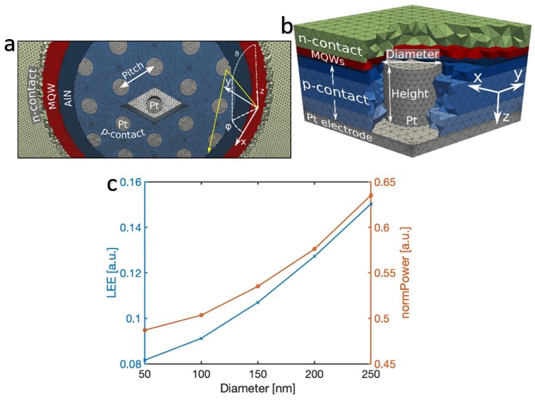
Figure 8. The optimization effect of the platinum (Pt) micropore hexagonal periodic structure on LEE in ultraviolet LEDs is illustrated in Fig.(a) Top-view schematic showing a hexagonal periodic array of Pt-filled micropores embedded in the p-type contact layer (pitch ≈ 300 nm). This structure disrupts total internal reflection, enhancing light scattering. (b) Three-dimensional structural illustration depicting the vertical distribution of the micropores (height ≈ 140 nm) and the Pt electrode filling, which reduces UV absorption and increases reflection (c) The variation of LEE and normalized emitted power (normPower) as a function of micropore diameter. When the diameter increases to 250 nm, LEE reaches 0.15 a.u. and the normalized power rises to 0.65 a.u., confirming the effectiveness of this structural optimization[81].
Furthermore, optimizing the chip sidewall morphology—such as by cutting bevels or applying optical polishing—and employing internal high-reflectivity mirrors or distributed Bragg reflectors (DBRs) are common approaches to enhance LEE. For instance, depositing nanoscale Ni reflective layers and Al layers beneath the p-type electrode significantly improves the device’s backward reflectance[2]. Additionally, optical designs at the packaging level, including silicone lenses, collimation structures, and microlens arrays, can effectively broaden the emission beam angle and increase the emitting area, thereby comprehensively optimizing the light extraction efficiency from a system perspective[2,37]. In summary, the design and integration of multiple optical structures represent a critical pathway for enhancing the EQE of UV LEDs.
3.6. Novel Structures and Approaches
In recent years, various innovative designs have emerged. Regarding polarization control, several studies have investigated semi-polar/non-polar epitaxy and surface plasmonic structures to modify the emission polarization distribution. Biomimetic microstructures, such as moth-eye-inspired nanostructured anti-reflection arrays, have been employed to further reduce surface reflection. For transparent electrodes, some groups have attempted to replace conventional Ni/Au contacts with transparent conductive oxides (TCOs) like ITO and ZnO, graphene nitride, or electrodeposited metal nanonets to minimize ultraviolet light absorption losses[82,83]. Additionally, advanced microfabrication techniques have drawn attention, such as micro-LED arrays and metamaterial-based surface plasmonic designs, which focus and enhance the emission beam to achieve significant LEE improvements[84].
Feng et al. reported the fabrication of 3 μm-pixel micro-LED arrays operating at 270 nm wavelength using high-precision microfabrication, achieving an EQE of 5.7% and a peak brightness of 396 W/cm² on the 3 μm devices[85]. Due to their small dimensions[86,87], micro-LEDs exhibit uniform current distribution and superior heat dissipation, resulting in higher LEE and power density[85]. Figure 9 compares the EQE and optical power density performance of deep ultraviolet micro-LEDs with different sizes: Figure 9(a) shows that the 3×3 μm² micro-device reaches a peak EQE of 5.7% at 70 A/cm² current density—significantly higher than the <2% EQE of the 100×100 μm² device—and maintains an EQE of 4.5% even when the current density increases to 4000 A/cm², indicating that miniaturization alleviates current crowding and thermal effects. Figure 9(b) demonstrates that the 3×3 μm² device achieves an optical power density of 396 W/cm² at 4000 A/cm², far surpassing the <100 W/cm² of the 100×100 μm² device, with power density increasing linearly with current density. These data directly support the experimental conclusion of 5.7% EQE and 396 W/cm² peak brightness for the 3 μm devices, highlighting the critical role of miniaturization in overcoming efficiency bottlenecks in deep ultraviolet LEDs. These novel approaches provide promising pathways to break through the efficiency limits of deep ultraviolet LEDs.
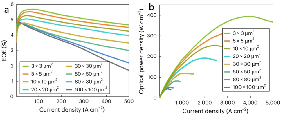
Figure 9. (a) A 3×3 μm² micro-LED achieves an EQE of 5.7% at a current density of 70 A/cm², significantly outperforming larger devices with EQE around 2%. However, the efficiency decreases rapidly as current increases due to limited heat dissipation caused by the small device size. (b) This micro-LED attains an optical power density of 396 W/cm² at 4000 A/cm² current density, benefiting from its small size and high current density, whereas larger devices tend to experience power saturation under high current injection[85].
4. Advances in the Application of GaN for Light Extraction Enhancement and Integrated Devices
With the increasing deployment of AlGaN-based DUV LEDs in high-power-density and long-term continuous operation applications, thermal management and device reliability have become critical concerns. Due to the relatively low EQE of DUV LEDs, a significant portion of the input power is converted into heat and accumulates within the chip, leading to elevated junction temperatures. This temperature rise exacerbates material defects, accelerates device degradation, and reduces light emission efficiency. Effectively reducing the device thermal resistance not only helps control the junction temperature and improve optical output but also extends the device lifetime. Therefore, establishing efficient thermal dissipation pathways and enhancing thermal stability are key challenges in the structural design and packaging processes of DUV LEDs. This chapter systematically discusses the main strategies and recent advances in reducing thermal resistance and improving device reliability from four perspectives: material modification, thermal interface materials, heat dissipation structure design, and packaging technology.
4.1. Material Modification
Using high thermal conductivity materials as chip substrates or packaging boards is an effective approach to improve the thermal management performance of DUV LEDs. Replacing sapphire substrates with single-crystal AlN substrates can significantly reduce thermal resistance and enhance device heat dissipation. The thermal conductivity of AlN ranges from 170 to 230 W/m·K, approximately nine times higher than that of sapphire, enabling faster and more uniform heat spreading. Lv et al. introduced a thermally oxidized Al₂O₃ layer within the device structure to improve the thermal performance of phototransistors, providing valuable insights for thermal interface optimization in DUV LEDs[88,89].Besides AlN, materials with even higher thermal conductivities such as silicon nitride (Si₃N₄), SiC, and diamond have also been extensively studied, especially for substrate designs in high-power devices. Tajima et al. demonstrated a multi-junction LED structure on a GaN-on-Si platform, highlighting its potential for high-power deep ultraviolet LEDs[90].In terms of material design, doping with specific elements such as carbon or oxygen, or constructing nanocomposite structures, has been employed to enhance the thermal conductivity of epitaxial layers and suppress defect propagation. For example, the incorporation of Ga₂O₃ sidewall layers in device structures can effectively reduce thermal accumulation, thereby improving device thermal stability and reliability. Additionally, optimizing the thermal conduction at the interface between the chip and substrate is equally crucial. The use of high-thermal-conductivity interface materials, such as metallized thermal grease and silver ceramic adhesives, can significantly enhance heat dissipation efficiency. Zhang et al. reported that SiC-enhanced copper-based composites exhibit excellent thermal conductivity, making them promising materials for packaging-level thermal management[91].
4.2. Application of GaN in Full-Color Micro-LED Displays
Thermal interface materials (TIMs) fill the gaps between the device chip and the heat dissipation substrate, acting as a crucial thermal conduction bridge. High-performance TIMs typically consist of silicone grease or composite materials embedded with thermally conductive ceramic particles such as boron nitride (BN), Al₂O₃, and SiO₂. Selecting TIMs with high thermal conductivity and low thermal resistance effectively reduces the overall thermal resistance of the LED packaging.Liu et al. demonstrated that silicone encapsulation frames exhibit excellent thermal stability in UVB LEDs[92]. Meanwhile, graphene-silver composite materials used as TIMs have been shown to reduce thermal resistance by over 20%[93]. Besides thermal performance, TIMs must also maintain electrical insulation and mechanical flexibility to prevent device failure. Recently, Li et al. provided a comprehensive review of thermal management from the packaging to system level, which helps in systematically understanding TIM optimization strategies[94].In UV LED packaging, common approaches to optimize TIM performance include controlling TIM thickness, applying proper compression techniques, and curing methods. Replacing thick soft gels with thin, highly thermally conductive materials significantly improves heat dissipation.Figure 10 illustrates thermal resistance test data highlighting the effectiveness of using AlN substrates combined with eutectic bonding processes. At an injection current of 200 mA, the packaging thermal resistance (from chip to substrate surface) decreased to 4.615 K/W, representing a 53%–85% reduction compared to conventional packaging methods (9.9 to 32 K/W). This result confirms that substituting organic substrates with high thermal conductivity AlN and replacing thick adhesive layers with thin metal eutectic bonds dramatically reduce interface thermal resistance and material thermal diffusion resistance. Consequently, the chip junction temperature can be lowered by more than 6.3 K according to theoretical calculations. This aligns with previous findings that silver sintering materials reduce junction temperature by tens of degrees, providing critical experimental support for heat dissipation design and TIM optimization in high-power UVB LEDs[37].
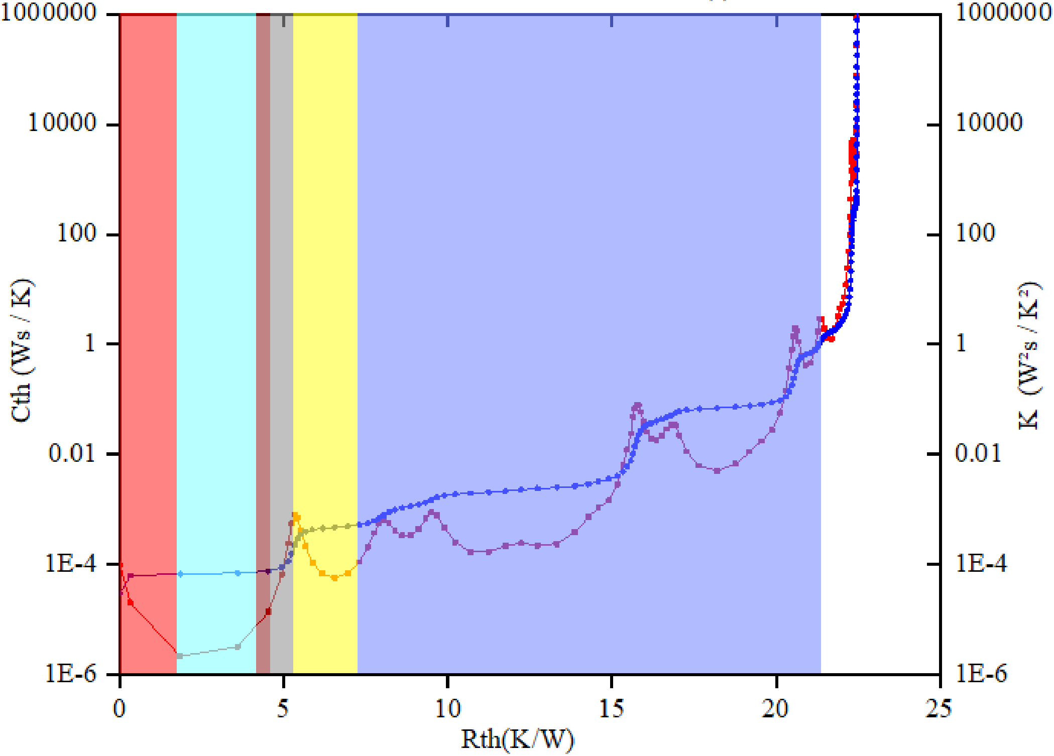
Figure 10. UVB LED package thermal resistance measurement[37]. The red region (left side) represents the low thermal resistance zone (Rth < 5 K/W), corresponding to highly efficient heat dissipation materials such as silver sintering sheets and boron nitride composites.The light blue region (middle) indicates the medium thermal resistance zone (5–15 K/W), which may correspond to conventional silicone grease or aluminum oxide-filled materials.The yellow/brown region (right side) denotes the high thermal resistance zone (Rth > 15 K/W), typically associated with low-performance organic adhesives or unoptimized interfaces.
4.3. Thermal Management Structure Design
Effective thermal management design is fundamental to ensuring reliable operation of LEDs. Common approaches include: (1)Flip-chip packaging and flip-chip structures, where the LED chip is mounted upside down on the substrate, exposing the emission side outward while placing the front electrode in direct contact with a high-thermal-conductivity heat sink, significantly shortening the heat flow path[2,37]; (2)Metal-core PCBs (MCPCB) or ceramic substrate packages that embed high thermal conductivity metals such as copper within the PCB core layer, allowing direct contact between the back side and the heat sink to improve heat dissipation efficiency; (3)Microchannel liquid cooling or heat pipe technologies, where LED arrays are fixed on heat sinks with microchannels, and circulating coolant removes substantial heat; (4)Optimizing lamp cup and lens structures to participate in heat dissipation by using high thermal conductivity plastics or metal mirrors instead of traditional epoxy glass; (5)Incorporating embedded heat dissipation structures such as copper or aluminum pillars within the package substrate to form three-dimensional thermal conduction paths.Liu et al. reported an optimized package design with specific length-to-width-to-height ratios, achieving a package thermal resistance as low as 4.6 K/W at 200 mA operation[37]. Additionally, researchers have explored synergistic designs combining wavy copper fins with liquid cooling systems to further enhance heat dissipation efficiency[95,96]. Moreover, fixing chips in stackable arrays with multiple submodules can improve overall thermal stability and prevent localized thermal overloads.
4.4. Packaging Technology
Packaging technology profoundly influences the reliability of UV LEDs. On one hand, a robust package provides physical protection to the chip, offering mechanical support and chemical stability. On the other hand, the packaging configuration (e.g., flip-chip, side-emitting, flip-chip side-emitting) and the choice of materials (substrates, fillers, encapsulants) are directly related to thermal dissipation and optical performance.In the ultraviolet spectral range, conventional epoxy encapsulants exhibit high absorption of UV light. Therefore, packaging materials must be selected for UV transparency or flame-retardant fluoropolymer-based resins. Recently developed nano-silver sintering interconnect structures have demonstrated excellent thermal conductivity and mechanical stability[97,98]. Moreover, avoiding excessive heat during soldering and using lead-free solder paste can reduce thermal damage to the chip.Innovative packaging structures such as vertical LED packaging (including matrix or pillar arrays) and modular array packaging have made significant progress in improving output power and reliability[99]. Additionally, when multiple LEDs operate in series or parallel, it is essential to consider uniform heat dissipation and driving schemes to ensure reliability.Packaging design directly impacts LED thermal management and reliability. High thermal conductivity packaging materials—such as thermally conductive ceramics and polymer composites—and high-performance TIMs like thermal adhesives, carbon nanotubes, or silver-based composites are commonly used to reduce thermal resistance. Studies have shown that employing diamond substrates or diamond thin films as heat spreaders can significantly extend the lifetime of high-power LEDs[100].Figure 11 compares two high-power LED packaging structures: MPLF (metal-plastic laminate frame) and MLF (full metal frame). Both use highly thermally conductive silver paste and Sn-pattern circuits. However, the (MLF) Figure 11(b) reduces the number of packaging layers by eliminating plastics and integrating a metal substrate, thus lowering the risk of thermal damage from soldering. The physical image of the MLF package demonstrates its miniaturized and integrated design (approximately 5×5 mm), suitable for high power density applications such as UV curing. This validates the advantages of full metal packaging in enhancing heat dissipation efficiency and reliability, achieving a 50% extension in device lifetime. Through structural innovation and integration of high thermal conductivity materials, the MLF package effectively reduces thermal resistance and prolongs device longevity, providing a critical technological pathway for deep ultraviolet LED packaging design.
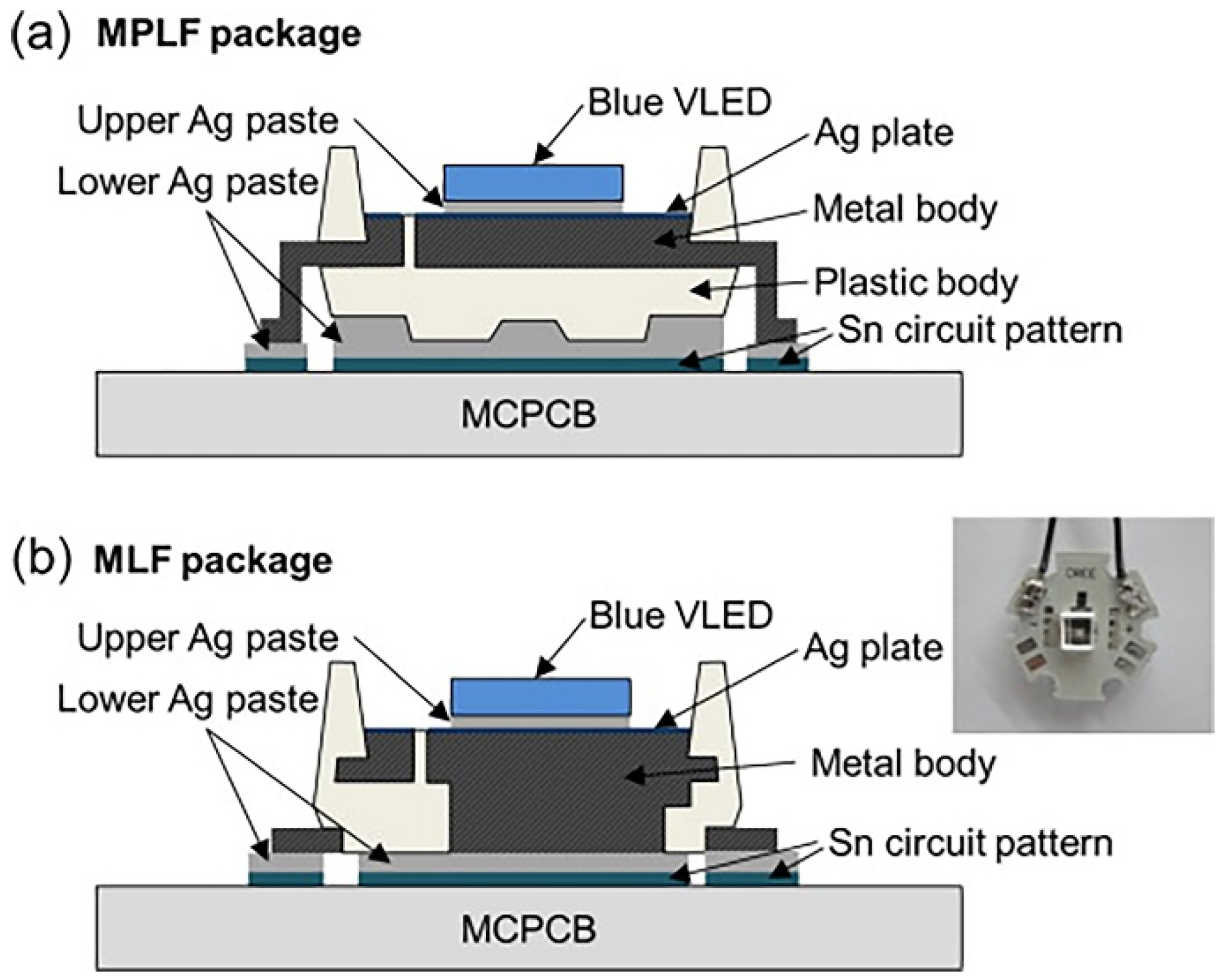
Figure 11. MPLF (Fig. a) includes a plastic body serving as an insulating layer; however, due to its low thermal conductivity (~0.2 W/m·K), it creates a thermal bottleneck, resulting in a relatively high thermal resistance of 6.8 K/W. In contrast, MLF (Fig. b) eliminates the plastic body and employs an all-metal structure (metal body), reducing the thermal resistance to 4.6 K/W. Additionally, the use of silver paste (Ag paste) for direct bonding of the vertical-cavity surface-emitting laser (Blue VLED) to the metal substrate (MCPCB) optimizes the heat dissipation path[44].
In summary, the combination of high thermal conductivity materials, optimized thermal interfaces, innovative heat dissipation structures, and packaging processes tailored for UV applications are key measures to reduce thermal resistance and extend the lifetime of AlGaN UV LEDs[44,101].
5. Conclusion and Outlook
GaN-based DUV LEDs show strong potential in public health, industrial inspection, and ultraviolet communication. However, their widespread commercialization remains limited by challenges such as low quantum efficiency, insufficient thermal management, and short device lifetime.
This review systematically analyzes the core bottlenecks in AlGaN-based DUV LEDs from the perspectives of epitaxial growth, device architecture, and fabrication techniques. Particular emphasis is placed on strategies to improve quantum efficiency and thermal performance, including quantum well and tunnel junction design[102], polarization engineering[103], high-quality heteroepitaxy[104], and interface optimization.
Moving forward, we propose that the future development of DUV LED technology should prioritize the following directions:
(1) development of low-defect, large-area AlN substrates to enable high-quality growth[105];
(2) integration of advanced packaging and thermal management systems featuring high thermal conductivity and low thermal resistance for high-power applications[106];
(3) realization of compact, integrated UV light modules for applications such as maskless lithography, wearable electronics, and biochips[107,108];
(4) in-depth studies on polarization fields, defect-related recombination, and non-radiative processes to support theoretical and material breakthroughs[108].
Furthermore, recent progress in strain engineering[109], quantum dot-based active regions[110], and surface passivation techniques[111] highlights additional pathways for enhancing device performance. With continued advances in materials science, micro/nano-fabrication, and system-level integration[108], GaN-based DUV LEDs are expected to play an increasingly central role in next-generation ultraviolet optoelectronics.
Conflicts of Interest
The authors declare no conflict of interest.
Author Contributions
Jiaxing Tang is the first author and contributed to the conception and writing of the manuscript. Zhe Lv, Yuanzhe Wang, and Ling Yang assisted with data and figures. Zhongxin Wu provided chemical materials. Jianfei Li and Jiancai Leng, as corresponding authors, supervised the project and revised the final manuscript.
Acknowledgements
This work was supported by the Jinan City-University Collaborative Development Strategy Project (Grant No. JNSX2023044). There is no conflict of interest in this paper. All the achievements of others have been properly cited.
References
-
M. Maraj, M. Li, W. H. Sun. "Reliability Analysis of AlGaN-Based Deep UV-LEDs." Nanomaterials. 2022, 12, 21, 3731.
-
M. Khan, N. Maeda, J. Yun, M. Jo, Y. Yamada, H. Hirayama. "Achieving 9.6% efficiency in 304nm p-AlGaN UVB LED via increasing the holes injection and light reflectance." Scientific Reports. 2022, 12, 2591.
-
K. Torii, A. Morita. "UVB irradiation induces HMGB1 expression in keratinocytes without promoting apoptosis." Exp. Dermatol. 2016, 25, 9, 741-742.
-
M. Kneissl, J. Rass, III-Nitride Ultraviolet Emitters, Technology and Applications, Springer, Cham, 2016.
-
S. Matsuura, S. Ishikura. "Suppression of Tomato mosaic virus disease in tomato plants by deep ultraviolet irradiation using light-emitting diodes." Lett. Appl. Microbiol. 2014, 59, 5, 457-463.
-
M. A. Khan, Y. Itokazu, N. Maeda, M. Jo, Y. Yamada, H. Hirayama. "External quantum efficiency of 6.5% at 300 nm emission and 4.7% at 310 nm emission on bare wafer of AlGaN-based UVB LEDs." ACS Appl. Electron. Mater. 2020, 2, 7, 1892-1907.
-
T. A. Kalajian, A. Aldoukhi, A. J. Veronikis, K. Persons, M. F. Holick. "Ultraviolet B light emitting diodes (LEDs) are more efficient and effective in producing vitamin D3 in human skin compared to natural sunlight." Sci. Rep. 2017, 7, 11489.
-
H. B. Yu, M. H. Memon, D. H. Wang, Z. J. Ren, H. C. Zhang, C. Huang, M. Tian, H. D. Sun, S. B. Long. "AlGaN-based deep ultraviolet micro-LED emitting at 275 nm." Opt. Lett. 2021, 46, 13, 3271-3274.
-
M. Kneissl, T. Y. Seong, J. Han, H. Amano. "The emergence and prospects of deep-ultraviolet light-emitting diode technologies." Nat. Photonics. 2019, 13, 233-244.
-
R. Q. Xu, Q. S. Kang, Y. W. Zhang, X. L. Zhang, Z. H. Zhang. "Research Progress of AlGaN-Based Deep Ultraviolet Light-Emitting Diodes." Micromachines. 2023, 14, 4, 844.
-
F. Z. Liang, M. X. Feng, Y. N. Huang, X. J. Sun, X. N. Zhan, J. X. Liu, Q. Sun, R. X. Wang, X. T. Ge, J. Q. Ning, H. Yang. "AlGaN-based Schottky barrier deep ultraviolet photodetector grown on Si substrate." Opt. Express. 2020, 28, 12, 17188-17195.
-
H. So, J. Lim, A. J. Suria, D. G. Senesky. "Highly antireflective AlGaN/GaN ultraviolet photodetectors using ZnO nanorod arrays on inverted pyramidal surfaces." Appl. Surf. 2017, 409, 91-96.
-
E. Monroy, F. Calle, J. L. Pau, E. Muñoz, F. Omnès, B. Beaumont, P. Gibart. "AlGaN-based UV photodetectors." J. Cryst. Growth. 2001, 230, 3-4, 537-543.
-
C. Pernot, A. Hirano, M. Iwaya, T. Detchprohm, H. Amano, I. Akasaki. "Low-Intensity Ultraviolet Photodetectors Based on AlGaN." Jpn. J. Appl. Phys. 1999, 38, 5A, L487-L489.
-
M. H. Crawford. "Materials Challenges of AlGaN-Based UV Optoelectronic Devices." Academic Press. 2017, 96, 3-44.
-
T. Y. Wang, C. T. Tasi, C. F. Lin, D. S. Wuu. "85% internal quantum efficiency of 280-nm AlGaN multiple quantum wells by defect engineering." Scientific Reports. 2017, 7, 14422.
-
Y. J. Song, R. He, J. X. Ran, J. X. Wang, J. M. Li, T. B. Wei. "III-nitride-based monolithic integration: From electronics to photonics." Appl. Phys. Rev. 2025, 12, 2, 021301.
-
L. Goswami, N. Aggarwal, M. Singh, R. Verma, P. Vashishtha, S. K. Jain, J. Tawale, R. Pandey, G. Gupta. "GaN Nanotowers Grown on Si (111) and Functionalized with Au Nanoparticles and ZnO Nanorods for Highly Responsive UV Photodetectors." ACS Appl. Nano Mater. 2020, 3, 8, 8104-8116.
-
X. J. Qiu, Y. D. Chen, E. Z. Han, Z. S. Lv, Z. Y. Song, H. Jiang. "High doping efficiency in p-type Al-rich AlGaN by modifying the Mg doping planes." Mater. Adv. 2020, 1, 77-85.
-
T. Y. Wang, W. C. Lai, S. Y. Sie, S. P. Chang, Y. R. Wu, Y. Z. Chiou, C. H. Kuo, J. K. Sheu. "AlGaN-based deep ultraviolet light emitting diodes with magnesium delta-doped AlGaN last barrier." Appl. Phys. Lett. 2020, 117, 251101.
-
C. Bayram, J. L. Pau, R. McClintock, M. Razeghi. "Delta-doping optimization for high quality p-type GaN." J. Appl. Phys. 2008, 104, 083512.
-
J. Simon, V. Protasenko, C. Lian, H. Xing, D. Jena. "Polarization-Induced Hole Doping in Wide-Band-Gap Uniaxial Semiconductor Heterostructures." Science. 2010, 327, 5961, 60-64.
-
J. C. Li, W. H. Yang, S. P. Li, H. Y. Chen, D. Y. Liu, J. Y. Kang. "Enhancement of p-type conductivity by modifying the internal electric field in Mg- and Si-δ-codoped AlxGa1−xN/AlyGa1−YN superlattices." Appl. Phys. Lett. 2009, 95, 151113.
-
M. Martens, C. Kuhn, E. Ziffer, T. Simoneit, V. Kueller, A. Knauer, J. Rass, T. Wernicke, S. Einfeldt, M. Weyers, M. Kneissl. "Low absorption loss p-AlGaN superlattice cladding layer for current-injection deep ultraviolet laser diodes." Appl. Phys. Lett. 2016, 108, 151108.
-
A. Pandey, X. Liu, Z. Deng, W. J. Shin, D. A. Laleyan, K. Mashooq, E. T. Reid, E. Kioupakis, P. Bhattacharya. "Enhanced doping efficiency of ultrawide band gap semiconductors by metal-semiconductor junction assisted epitaxy." Phys. Rev. Mater. 2019, 3, 053401.
-
M. A. Khan, J. P. Bermundo, Y. Ishikawa, H. Ikenoue, S. Fujikawa, E. Matsuura, Y. Kashima, N. Maeda, M. Jo, H. Hirayama. "Impact of Mg level on lattice relaxation in a p-AlGaN hole source layer and attempting excimer laser annealing on p-AlGaN HSL of UVB emitters." Nanotechnology. 2020, 32, 5, 055702.
-
Z. Q. Liu, X. Y. Yi, L. C. Wang, T. B. Wei, G. D. Yuan, J. C. Yan, J. X. Wang, J. M. Li, Y. Shi, Y. Zhang. "Impurity resonant state p-doping layer for high-efficiency nitride-based light-emitting diodes." Semicond. Sci. Technol. 2018, 33, 11, 114004.
-
Y. W. Zhang, Degree Thesis, Ohio State University, 2018.
-
Y. Taniyasu, M. Kasu, T. Makimoto. "An aluminium nitride light-emitting diode with a wavelength of 210 nanometres." Nature. 2006, 441, 325-328.
-
A. Khan, K. Balakrishnan, T. Katona. "Ultraviolet light-emitting diodes based on group three nitrides." Nat. Photonics. 2008, 2, 77-84.
-
S. Zhao, H. P. T. Nguyen, M. G. Kibria, Z. Mi. "III-Nitride nanowire optoelectronics." Prog. Quantum Electron. 2015, 44, 14-68.
-
Y. W. Cao, Q. J. Lv, T. P. Yang, T. T. Mi, X. W. Wang, W. Liu, J. L. Liu. "Realization of high-efficiency AlGaN deep ultraviolet light-emitting diodes with polarization-induced doping of the p-AlGaN hole injection layer." Chin. Phys. B. 2023, 32, 5, 058503.
-
P. Yang, L. J. Kong, N. Gao, S. P. Li, J. Y. Kang, R. Zhang. "Enhancing performance of AlGaN deep-UV LEDs by p-Al0.6Ga0.4N/p-GaN thin-wells superlattice as hole injection layer." Physica Scripta. 2025, 100, 3, 035528.
-
A. X. Zhang, Z. Q. Xing, Y. P. Qu, F. Wang, J. Liou, Y. H. Liu. "Optimization of AlGaN-based deep ultraviolet light emitting diodes with superlattice step doped electron blocking layers." Optics Express. 2024, 32, 6, 10146-10157.
-
D. Myren, F. Vásquez-Aza, J. S. Lundh, M. J. Tadjer, G. Pavlidis. "Emerging thermal metrology for ultra-wide bandgap semiconductor devices." Appl. Phys. Lett. 2025, 126, 200502.
-
P. Manley, S. Walde, S. Hagedorn, M. Hammerschmidt, S. Burger, C. Becker. "Nanopatterned Sapphire Substrates in Deep-UV LEDs: Is there an Optical Benefit?" Opt. Express. 2020, 28, 3, 3619-3635.
-
C. N. Liu, C. C. Hu, Y. J. Zheng, Y. F. Hsu, Z. T. Ye. "Packaged structure optimization for enhanced light extraction efficiency and reduced thermal resistance of ultraviolet B LEDs." Optics Express. 2024, 32, 7, 12438-12448.
-
Z. H. Zhang, S. W. H. Chen, C. S. Chu, K. K. Tian, M. Q. Fang, Y. H. Zhang, W. G. Bi, H. C. Kuo. "Nearly efficiency-droop-free AlGaN-based ultraviolet light-emitting diodes with a specifically designed superlattice p-type electron blocking layer for high Mg doping efficiency." Nanoscale Research Letters. 2018, 13, 122.
-
S. Q. Lu, Z. Y. Luo, J. C. Li, W. Lin, H. Y. Chen, D. Y. Liu, D. J. Cai, K. Huang, N. Gao, Y. H. Zhou, S. P. Li, J. Y. Kang. "Role of Strain-Induced Microscale Compositional Pulling on Optical Properties of High Al Content AlGaN Quantum Wells for Deep-Ultraviolet LED." Nanoscale Res. Lett. 2022, 17, 13.
-
A. Pandey, W. J. Shin, J. Gim, R. Hovden, Z. Mi. "High-efficiency AlGaN/GaN/AlGaN tunnel junction ultraviolet light-emitting diodes." Photonics Res. 2020, 8, 3, 331-337.
-
L. Li, Y. Miyachi, M. Miyoshi, T. Egawa. "Ultrathin inserted AlGaN/InAlN heterojunction for performance improvement in AlGaN-based deep ultraviolet light-emitting diodes." Applied Physics Express. 2019, 12, 1, 011010.
-
M. N. Sharif, M. Usman, M. I. Niass, J. J. Liou, F. Wang, Y. H. Liu. "Compositionally graded AlGaN hole source layer for deep-ultraviolet nanowire light-emitting diode without electron blocking layer." Nanotechnology. 2021, 33, 7, 34438377.
-
G. Zhang, J. W. Pomeroy, M. E. Navarro, H. Cao, M. Kuball, Y. Ding. "3-D Printed Microjet Impingement Cooling for Thermal Management of Ultrahigh-Power GaN Transistors." IEEE Xplore. 2021, 11, 5, 748-754.
-
P. H. Liu, C. H. She, L. P. Tan, P. P. Xu, L. Yan. "Development of LED Package Heat Dissipation Research." Micromachines. 2022, 13, 2, 229.
-
C. C. Hu, Y. J. Zheng, C. N. Liu, Z. T. Ye. "Full-angle chip scale package of mini LEDs with V-shape packaging structure." Opt. Express. 2024, 32, 6, 9287-9296.
-
S. Khandekar, G. Sahu, K. Muralidhar, E. Y. Gatapova, O. A. Kabov, R. Hu, X. B. Luo, L. Zhao. "Cooling of high-power LEDs by liquid sprays: Challenges and prospects." Appl. Therm. Eng. 2021, 184, 115640.
-
Z. T. Ye, C. C. Hu, Y. J. Zheng. "Wide heart-shaped mini-LEDs without a second lens as a large area, ultra-high luminance, and flat light source." Opt. Express. 2024, 32, 4, 5874-5884.
-
M. Azarifar, C. Cengiz, M. Arik. "Thermal and optical performance characterization of bare and phosphor converted LEDs through package level immersion cooling." Int. J. Heat Mass Transfer. 2022, 189, 122607.
-
T. Luo, Y. Tong, J. C. Lu, Y. Mou, Q. Wang, J. X. Liu. "Enhanced Optical-Thermal Performances of High-Power LED by Plated Copper on Thick Film Ceramic Substrate." IEEE Trans. Electron. Devices. 2023, 70, 7, 3774-3779.
-
Y. X. Chen, J. W. Ben, F. J. Xu, J. C. Li, Y. Chen, X. J. Sun, D. B. Li. "Review on the Progress of AlGaN-based Ultraviolet Light-Emitting Diodes." Fundamental Research. 2021, 1, 6, 717-734.
-
D. Cameron, P. Edwards, F. Mehnke, G. Kusch. "The influence of threading dislocations propagating through an AlGaN UVC LED." Appl. Phys. Lett. 2022, 120, 16, 162101.
-
R. Samani, I. G. Zurbriggen, R. Y. Hou, J. C. Lu, A. M. Knight. "Comprehensive System-Level Thermal Performance and Power Density Optimization in Enclosed Natural Convection PFC-LLC GaN Converters." IEEE Xplore 2025, 61, 2, 3371-3383.
-
S. U. Khan, Y. Wang, A. X. Zhang, S. M. Nawaz, M. I. Niass, F. Wang, Y. H. Liu. "AlGaN-Based Deep UV Laser Diodes without an Electron Blocking Layer and with a Reduced Aluminum Composition of Quantum Barriers." Springer Nature 2022, 43, 694-701.
-
T. W. Lan, K. H. Su, C. C. Chang, C. L. Chen, C. L. Chen, M. N. Ou, D. Z. Wu, P. M. Wu, C. Y. Su, M. K. Wu, Y. Y. Chen. "Enhancing the figure of merit in thermoelectric materials by adding silicate aerogel." Mater. Today Phys. 2020, 13, 100215.
-
H. C. Wu, H. Li, S. Y. Kuo, B. Y. Chen, T. C. Lu, H. M. Huang. "High Output Power GaN-Based Green Resonant-Cavity Light-Emitting Diodes With Trapezoidal Quantum Wells." IEEE Xplore 2020, 67, 9, 3650-3654.
-
M. Y. Zhanghu, Y. B. Liu, B. R. Hyun, Y. F. Li, Z. J. Liu. "Optimizing InGaN Micro-LED Efficiency: Investigating the Internal Quantum Efficiency and Ideality Factor Connection." IEEE Xplore 2024, 71, 10, 6190-6197.
-
Y. C. Tsai, C. Bayram, J. P. Leburton. "Interplay between Auger recombination, carrier leakage, and polarization in InGaAlN multiple-quantum-well light-emitting diodes." J. Appl. Phys. 2022, 131, 193102.
-
W. H. Yang, J. C. Li, Y. Zhang, P. K. Huang, T. C. Lu, H. C. Kuo, S. P. Li, X. Yang, H. Y. Chen, D. Y. Liu, J. y. Kang. "High density GaN/AlN quantum dots for deep UV LED with high quantum efficiency and temperature stability." Sci. Rep. 2014, 4, 5166.
-
R. C. Subedi, J. W. Min, S. Mitra, K. H. Li, I. Ajia, E. Stegenburgs, D. H. Anjum, M. Conroy, K. Moore, U. Bangert, I. S. Roqan, T. K. Ng, B. S. Ooi. "Quantifying the Transverse-Electric-Dominant 260 nm Emission from Molecular Beam Epitaxy-Grown GaN-Quantum-Disks Embedded in AlN Nanowires: A Comprehensive Optical and Morphological Characterization." ACS Appl. Mater. Interfaces 2020, 12, 37, 41649–41658.
-
M. Wang, F. Wu, Y. F. Yao, C. Zollner, M. Lza, M. Lam, S. P. Denbaars, S. J. Nakamura, J. S. Speck. "10.6% external quantum efficiency germicidal UV LEDs grown on thin highly conductive n-AlGaN." Appl. Phys. Lett. 2023, 123, 231101.
-
Z. X. Yuan, Y. Z. Li, X. Y. Lu, Z. Wang, P. J. Qiu, X. G. Cui. "Investigation of Modulation Bandwidth of InGaN Green Micro-LEDs by Varying Quantum Barrier Thickness." IEEE Xplore 2022, 69, 8, 4298-4305.
-
M. B. Ben Hamida, M. Hatami. "Optimization of fins arrangements for the square light emitting diode (LED) cooling through nanofluid-filled microchannel." Sci. Rep. 2021, 11, 12610.
-
S. Liang, R. Hao, D. Fan, B. Li, J. Huang, Y. Zhang, J. Wu, Y. Li, J. Mo. "Structural optimization and numerical thermal analysis of ultraviolet light-emitting diodes with high-power multi-chip arrays." Optik 2020, 222, 165333.
-
N. Fiuczek, M. Sawicka, A. F. Żmuda, M. Siekacz, M. Żak, K. N. Szkudlarek, G. Muzioł, P. Wolny, J. J. Kelly, C. Skierbiszewski. "Electrochemical etching of p-type GaN using a tunnel junction for efficient hole injection." Acta Mater. 2022, 234, 1, 118018.
-
E. R. Cardozo, A. Naranjo, A. Pfenning, V. Lopez-richard, G. E. Marques, L. Worschech, F. Hartmann, S. Hofling, M. D. Teodoro. "Determination of Carrier Density and Dynamics via Magnetoelectroluminescence Spectroscopy in Resonant-Tunneling Diodes." Phys. Rev. Appl. 2021, 15, 014042.
-
G. Q. Deng, J. Q. Yu, Y. F. Niu, L. D. Zhang, H. T. Ma, Y. Wang, C. C. Zuo, S. X. Yang, X. Han, L. Chen, B. L. Zhang, D. B. Li, Y. T. Zhang. "Demonstration of Full AlGaN Tunnel Junction Ultraviolet LED." ACS Photonics 2024, 11, 5, 1866–1872.
-
Y. M. Sang, D. Q. Zhang, Z. Zhang, J. C. Yu, F. F. Xu, D. Jiang. "Monolithic Integration of GaN-Based Green Micro-LED and Quasi-Vertical MOSFET Utilizing a Hybrid Tunnel Junction." IEEE Xplore 2023, 44, 7, 1156-1159.
-
S. U. Kim, D. Y. Um, J. K. Oh, B. Chandran, C. R. Lee, Y. H. Ra. "Structural Engineering in a Microscale Laser Diode with InGaN Tunnel-Junction Nanorods." ACS Photonics 2023, 10, 4, 1053–1059.
-
Z. Zhao, Y. Liu, P. X. Li, X. W. Zhou, B. Yang, Y. R. Xiang. "Enhanced Hole Injection in AlGaN-Based Ga-Polar Ultraviolet Light-Emitting Diodes with Polarized Electric-Field Reservoir Electron Barrier." Micromachines 2024, 15, 6, 38930732.
-
J. Hu, J. Zhang, Y. Zhang, H. Zhang, H. Long, Q. Chen, M. Shan, S. Du, J. Dai, C. Chen. "Enhanced Performance of AlGaN-Based Deep Ultraviolet Light-Emitting Diodes with Chirped Superlattice Electron Deceleration Layer." Nanoscale Res. Lett. 2019, 14, 347.
-
G. Guérin, F. Jourdan, J. L. Rouvière, B. Gayral, G. Jacopin, B. Daudin. "Optical properties of basal plane stacking faults in AlN nanowires." J. Appl. Phys. 2025, 137, 174303.
-
J. Bruckbauer, Y. P. Gong, L. Jiu, M. J. Wallace, A. Ipsen, S. Bauer, R. Müller, J. Bai, K. Thonke, T. Wang, C. T. Cowan, R. W. Martin. "Influence of micro-patterning of the growth template on defect reduction and optical properties of non-polar (1120) GaN." Appl. Phys. 2021, 54, 2, 025107.
-
J. Tatebayashi, T. Otabara, T. Yoshimura, R. Hada, R. Yoshida, S. Ichikawa, Y. Fujiwara. "Formation and Optical Characteristics of GaN:Eu/GaN Nanowires for Applications in Light-Emitting Diodes." ECS J. Solid State Sci. Technol. 2023, 12, 9, 096003.
-
C. Y. Zhang, K. Jiang, X. J. Sun, D. B. Li. "Recent Progress on AlGaN Based Deep Ultraviolet Light-Emitting Diodes below 250 nm." Crystals 2022, 12, 12, 1812.
-
M. Kim, H. Jee, J. Lee. "Photo-Sintered Silver Thin Films by a High-Power UV-LED Module for Flexible Electronic Applications." Nanomaterials 2021, 11, 11, 2840.
-
I. Bryan, Z. Bryan, S. Washiyama, P. Reddy, B. Gaddy, B. Sarkar, M. Breckenridge, Q. Guo, M. Bobea, J. Tweedie, S. Mita, D. Lrving, R. Collazo, Z. Sitar. "Doping and compensation in Al-rich AlGaN grown on single crystal AlN and sapphire by MOCVD." Appl. Phys. Lett. 2018, 112, 062102.
-
M. H. Breckenridge, Q. Guo, A. Klump, B. Sarkar, Y. Guan, J. Tweedie, R. Kirste, S. Mita, P. Reddy, R. Collazo, Z. Sitar. "Shallow Si donor in ion-implanted homoepitaxial AlN." Appl. Phys. Lett. 2020, 116, 172103.
-
T. Kunimune, M. Kuramoto, S. Ogawa, T. Sugahara, S. Nagao, K. Suganuma. "Ultra thermal stability of LED die-attach achieved by pressureless Ag stress-migration bonding at low temperature." Acta Mater. 2022, 228, 118721.
-
H. L. Chang, Z. T. Liu, S. Y. Yang, Y. Q. Gao, J. Y. Shan, B. Y. Liu, J. Y. Sun, Z. L. Chen, J. C. Yan, Z. Q. Liu, J. X. Wang, P. Gao, J. M. Li, Z. F. Liu, T. B. Wei. "Graphene-driving strain engineering to enable strain-free epitaxy of AlN film for deep ultraviolet light-emitting diode." Light. Sci. Appl. 2022, 11, 119.
-
Z. H. Zhang, S. H. Chen, Y. H. Zhang, L. P. Li, S. W. Wang, K. K. Tian, C. S. Chu, M. Q. Fang, H. C. Kuo, W. G. Bi. "Hole transport manipulation to improve the hole injection for deep ultraviolet light-emitting diodes." Acs. Photonics. 2017, 4, 7, 1846–1850.
-
E. López-Fraguas, F. Binkowski, S. Burger, S. Hagedorn, B. García-Cámara, R. Vergaz, C. Becker, P. Manley. "Tripling the light extraction efficiency of a deep ultraviolet LED using a nanostructured p-contact." Scientific. Reports. 2022, 12, 11480.
-
S. Q. Lu, P. Shen, H. Y. Zhang, G. Z. Liu, B. Guo, Y. H. Cai, H. Chen, F. Y. Xu, T. C. Zheng, F. C. Xu, X. H. Chen, D. J. Cai, J. Y. Kang. "Towards n-type conductivity in hexagonal boron nitride." Nature. Communications. 2022, 13, 3109.
-
Y. F. Yang, Y. Peng, M. F. Saleem, Z. Q. Chen, W. H. Sun. "Hexagonal Boron Nitride on III–V Compounds: A Review of the Synthesis and Applications." Materials. 2022, 15, 13, 4396.
-
O. Segal, A. Shultzman, Y. Kurman, I. Kaminer. "Optimizing the spontaneous-emission of far-UVC phosphors." Appl. Phys. Lett. 2022, 120, 231902.
-
F. Feng, Y. B. Liu, K. Zhang, H. Yang, B. R. Hyun, K. Xu, H. S. Kwok, Z. J. Liu. "High-power AlGaN deep-ultraviolet micro-light-emitting diode displays for maskless photolithography." Nature. Photonics. 2024, 19, 1, 101-108.
-
L. Wang, L. M. Yu, Z. H. Li, A. D. Cheng, Z. B. Hao, C. Z. Sun, B. Xiong, Y. J. Han, J. Wang, H. T. Li, L. Gan, Y. Luo. "InGaN quantum dots for micro-LEDs." APL. Photonics. 2024, 9, 100904.
-
R. S. Hua, Z. W. Xu, Z. X. Tao, B. Dong, H. Wang, L. Yang. "Fabrication of high-quality surface microtextures on GaN by femtosecond laser direct writing." Nanotechnol. Precis. Eng. 2025, 8, 013005.
-
K. Fu, J. W. Fu, W. X. Wu, Z. Q. Ye, B. J. Wang, J. B. Yan, F. Shi, P. Z. Liu, Y. J. Wang. "Convolutional neural network-based simultaneous display-communication system." APL. Photonics. 2025, 10, 036108.
-
Z. S. Lv, T. Z. Peng, G. Wang, H. Jiang. "Substantial improvement of InGaN/GaN visible-light polarization-induced self-depletion phototransistor by thermally oxidized Al2O3." Appl. Phys. Lett. 2024, 125, 191104.
-
J. Tajima, H. Ono, T. Ito, K. Uesugi, S. Nunoue. "Fabrication and characteristics of high-power multijunction LEDs using GaN-on-Si technologies." Phys. Status. Solidi. A. 2016, 213, 5, 1177-1180.
-
Y. X. Zhang, L. Y. Lai, D. Y. Cui, Y. Zhu, H. Cai, B. Yan, Y. H. Li, Z. Q. Yang, G. F. Ding. "Hybrid effect on mechanical and thermal performance of copper matrix composites reinforced with SiC whiskers." Ceramics. International. 2024, 50, 9, 16553-16563.
-
T. Y. Liu, S. M. Huang, M. J. Lai, R. S. Liu, Y. T. Chang, W. H. Sun. "Epoxy Molding Compound Lead Frames With Silicone Resin for Encapsulating AlGaN-Based UVB Light-Emitting Diodes." IEEE. Xplore. 2021, 9, 129874-129880.
-
P. Ayush, M. Zetian. "III-Nitride Nanostructures for High Efficiency Micro-LEDs and Ultraviolet Optoelectronics." IEEE. Xplore. 2022, 58, 4, 1-13.
-
Z. T. Li, J. Tan, J. S. Li, X. R. Ding, Y. Tang. "A review on thermal management of light-emitting diodes: From package-level to system-level." Applied. Thermal. Engineering. 2024, 257, Part A, 124145.
-
B. C. Letson, S. Barke, P. Wass, G. Mueller, F. Ren, S. J. Pearton, J. W. Conklin. "Deep UV AlGaN LED reliability for long duration space missions." Vac. Sci. Technol. 2023, 41, 1, 013202.
-
M. A. Shah, D. G. Lee, S. Hur. "Design and Characteristic Analysis of a MEMS Piezo-Driven Recirculating Inkjet Printhead Using Lumped Element Modeling." Micromachines. 2019, 10, 11, 757.
-
M. S. Kim, K. Matsunaga, Y. H. Ko, C. W. Lee, H. Nishikawa. "Reliability of Ag Nanoporous Bonding Joint for High Temperature Die Attach under Temperature Cycling." Materials. Transactions. 2016, 57, 7, 1192-1196.
-
D. S. Yang, Y. L. Huang, Y. H. Tian. "Microstructure of Ag Nano Paste Joint and Its Influence on Reliability." Crystals. 2021, 11, 12, 1537.
-
H. W. Wang, P. F. Bai, H. Cui, X. T. Zhang, Y. F. Tang, S. Y. Liang, S. X. Li, G. F. Zhou. "Bioinspired thermally conducting packaging for heat management of high performance electronic chips." Communications. Engineering. 2025, 4, 1.
-
S. H. Lin, M. C. Tseng, R. H. Horng, S. Q. Lai, K. W. Peng, M. C. Shen, D. S. Wuu, S. Y. Lien, H. C. Kuo, Z. Chen, T. Z. Wu. "Thermal behavior of AlGaN-based deep-UV LEDs." Optics. Express. 2022, 30, 10, 16827-16836.
-
A. Hiraiwa, K. Horikawa, H. Kawarada. "Bias stability enhancement of metal/Al2O3/AlN/GaN capacitors by high-temperature plasma-enhanced atomic layer deposition of thin AlN interlayer." J. Vac. Sci. Technol. B. 2025, 43, 032205.
-
M. C. Shan, Y. Zhang, M. Tian, R. Y. Liu, J. A. Jiang, Z. H. Zheng, Y. M. Zhao, Y. Lu, Z. C. Feng, W. Guo, J. N. Dai, C. Q. Chen, F. Wu, X. H. Li. "Transverse Electric Lasing at a Record Short Wavelength 244.63 nm from GaN Quantum Wells with Weak Exciton Localization." ACS. Photonics. 2021, 8, 5, 1264-1270.
-
S. F. Liu, W. Luo, D. Li, Y. Yuan, W. Tong, J. J. Kang, Y. X. Wang, D. Li, X. Rong, T. Wang, Z. Y. Chen, Y. D. Li, H. J. Wang, W. Y. Wang, J. Hoo, L. Yan, S. P. Guo, B. Shen, Z. Cong, X. Q. Wang. "Sec-Eliminating the SARS-CoV-2 by AlGaN Based High Power Deep Ultraviolet Light Source." Advanced. Functional. Materials. 2020, 31, 7, 2008452.
-
F. Mehnke, X. T. Trinh, H. Pingel, T. Wernicke, E. Janzen, N. T. Son, M. Kneissl. "Electronic properties of Si-doped AlxGa1−xN with aluminum mole fractions above 80%." J. Appl. Phys. 2016, 120, 145702.
-
J. Y. Tsao, S. Chowdhury, M. A. Hollis, D. Jena, N. M. Johnson, K. A. Jones, R. J. Kaplar, S. Rajan, C. G. Vandewalle, E. Bellotti, C. L. Chua, R. Collazo, M. E. Coltrin, J. A. Cooper, K. R. Evans, S. Graham, T. A. Grotjohn, E. R. Heller, M. Higashiwaki, M. S. Islam, P. W. Juodawlkis, M. A. Khan, A. D. Koehler, J. H. Leach, U. K. Mishra, R. J. Nemanich, R. C. N. Pilawa-Podgurski, J. B. Shealy, Z. Sitar, M. J. Tadjer, A. F. Witulski, M. Wraback, and J. A. Simmons. "Ultrawide-Bandgap Semiconductors: Research Opportunities and Challenges." Adv. Electron. Mater. 2018, 4, 1, 1600501.
-
Y. J. Ding, L. L. Xu, Q. Wang, R. L. Liang, Y. Peng, X. Z. Wang, J. N. Dai, M. X. Chen. "Heat Dissipation Enhancement of High-Power Deep-Ultraviolet LEDs Through Plated Copper on Thick Film Diamond Substrates." IEEE. Electron. Device. Letters. 2024, 45, 9, 1634-1637.
-
F. Feng, Y. B. Liu, K. Zhang, M. Y. Zhanghu, K. W. Chan, K. Xu, H. S. Kwok, Z. J. Liu. "Enhancing the optical and electrical properties of AlGaN ultraviolet-C micro-LED via a hybrid scheme of plasma and chemical treatment." Appl. Phys. Lett. 2022, 121, 221104.
-
Z. Q. Ye, H. Zhang, X. M. Gao, K. Fu, H. B. Zeng, Y. H. Liu, Y. J. Wang, and H. Amano. "Simultaneous light emission and detection of an AlGaInP quantum well diode." AIP. Adv. 2023, 13, 045003.
-
X. M. Gao, P. Z. Liu, Q. X. Yin, H. Wang, J. W. Fu, F. R. Hu, Y. Jiang, H. B. Zhu, Y. J. Wang. "Wireless light energy harvesting and communication in a waterproof GaN optoelectronic system." Commun. Eng. 2022, 1, 16.
-
C. H. Kang, G. Y. Liu, C. M. Lee, O. Alkhazragi, J. M. Wagstaff, K. H. Li, F. Alhawaj, T. K. Ng, J. S. Speak, S. Nakamura, S. Nakamura, S. P. Denbaars, B. S. Ooi. "Semipolar (2021) InGaN/GaN micro-photodetector for gigabit-per-second visible light communication." Appl. Phys. Express. 2020, 13, 014001.
-
S. X. Tan, J. C. Zhang, T. Egawa, G. Chen. "Influence of quantum-well number and an AlN electron blocking layer on the electroluminescence properties of AlGaN deep ultraviolet light-emitting diodes." Appl. Sci. 2018, 8, 12, 2402.