Y-Shaped Topological Photonic Crystal Waveguide Design on Lithium Niobate for Integrated Beam Splitter and Combiner
published: 06 March 2025 | https://doi.org/10.63174/xdi-TPLP3530
Abstract
Photonic topological insulators offer promising solutions for realizing lossless light transmission through topological edge states and backscattering suppression, particularly in compact waveguide devices. In this work, a novel two-dimensional photonic crystal structure based on lithium niobate (LN) dielectric rods is designed and investigated. Through finite element method simulations, the band structure and topological properties were systematically analyzed by varying key geometric parameters. The simulation results demonstrated robust unidirectional light propagation at the interface between regions of different topological properties, with propagation direction controlled by the incident light polarization. Based on these properties, a Y-shaped waveguide structure was designed, showing efficient performance in both beam splitting and combining operations. The proposed structure, featuring simple geometric configuration and straightforward topological phase transition control, demonstrates significant potential for practical applications in integrated optical systems. This design approach provides an effective pathway for developing compact topological photonic devices with controlled light propagation characteristics.
1. Introduction
Lithium niobate (LN) integrated photonic technology has emerged as a cornerstone for high-speed and large-capacity data transmission, driven by significant advances in material science and integration technology.[1-3] The exceptional performance of LN-based integrated photonic circuits has been extensively demonstrated across diverse applications, including optical communications, laser radar systems, microwave photonics, and quantum optical devices.[4-6] Various fabrication techniques have been developed for LN integrated circuits, such as lithography, femtosecond laser micromachining, heterogeneous bonding, periodically poled lithium niobate (PPLN) film technology, and chemical mechanical polishing (CMP).[7-9] In recent years, photonic crystals, which utilize periodic modulation of electromagnetic waves to generate photonic bands and bandgaps, have presented a promising approach for integrated optoelectronic circuit design.[10-13] These structures can be categorized as one-, two-, or three-dimensional based on their spatial periodicity and bandgap characteristics. Among these, two-dimensional photonic crystals, consisting of periodically arranged dielectric rods or air holes, have garnered particular attention due to their practical applicability and versatile functionality.[14] Of special interest are their topological properties: when two photonic crystals with distinct topological band structures are interfaced, robust unidirectional light propagation occurs along their junction, independent of the interface geometry.[15-17] This unique characteristic enables high-quality signal transmission across specific optical communication bands, offering new possibilities for integrated photonic devices.[18-25]
Significant progress has been made in topological photonic devices in recent years. In 2019, researchers demonstrated a silicon-on-insulator (SOI) valley-topological photonic crystal slab waveguide that achieved transmission of valley-topological nanophotonic structures at communication wavelengths while maintaining in-plane robustness and optical constraints.[26] Subsequently, a topologically protected Mach-Zehnder interferometer (TPMZI) utilizing the valley Hall effect was developed in 2020, demonstrating robust photon transmission at interfaces despite sharp bends and defects, thereby ensuring high sensitivity and output power.[27] Further advances in 2021 combined topological photonics with quantum optics, resulting in an on-chip valley-dependent quantum information processing system featuring a fork-shaped beam splitter based on valley photonic crystal waveguides, which achieved high-visibility two-photon interference.[28] In 2025, researchers demonstrated a novel method for generating stable and vivid physical colors on the surface of LN crystals using the combination of metallic ion implantation and LDW technologies. The embedded Au nanoparticles altered the light-matter interaction system between the crystal lattices and the lasers, contributing to the generation of surface colors.[29] However, most existing designs require complex structures and precise fabrication processes, while the integration of multiple functions remains challenging.[30-32] There is a pressing need for simpler and more efficient topological photonic devices.
In this work, a novel two-dimensional photonic crystal structure based on LN dielectric rods is proposed, featuring straightforward geometric configuration and efficient topological phase transition control. By modulating the distance between unit dielectric rods, we demonstrate the opening of energy bands and topological phase transition, leading to the inversion of p and d states. The interface between two photonic crystals with different topological properties enables unidirectional light propagation due to the presence of helical edge states in the photonic bandgap. Based on these properties, we design and analyze a Y-shaped waveguide structure that functions as both a beam splitter and combiner. Our findings provide practical insights for developing integrated photonic devices through microfabrication processes, particularly for applications requiring robust light manipulation and multi-functional integration.
2. Theoretical Framework and Model Construction
The transverse magnetic field mode (TM wave) in a two-dimensional photonic crystal, where the magnetic field is parallel to the dielectric rod axis and has only the z-component (Hz), while the electric field lies in-plane with x-component (Ex) and y-component (Ey). From Maxwell's equations, we can derive that Hz satisfies the wave equation:
where $ \varepsilon_{r} $ and $ \mu_{r} $ are the relative permittivity and relative permeability, and $ c_{0} = 1/\sqrt{\varepsilon_{0}\mu_{0}} $ is the speed of light in vacuum or air. Like electronic crystals, two-dimensional photonic crystal structures are periodic. The solution of wave equation should satisfy Bloch theorem:
where $ u_{n\overset{\rightarrow}{k}}\left( \overset{\rightarrow}{r} \right) $ is a periodic function with the same periodicity as the lattice structure. The corresponding eigenfrequency of the Bloch function represented by the above formula is $ \omega_{n\overset{\rightarrow}{k}}$. The relationship between $ \omega_{n\overset{\rightarrow}{k}} $ and Bloch wave vector $ \overset{\rightarrow}{k} $ is the dispersion relationship. The orthogonal relationship satisfied by the Bloch wave function is:
where $ \Omega $ denotes the area of the unit cell, the integral is over the whole unit cell, and ${~\delta}_{ij}$ is the Kronecker function.
In this work, we designed a two-dimensional hexagonal honeycomb structure, as shown in Figure 1A. The cross-section of the circular LN dielectric rods is symmetrically arranged, and the cross-sectional center of each dielectric rod is located on the lattice of the hexagonal honeycomb structure. Therefore, a hexagonal honeycomb photonic crystal like the graphene lattice structure is constructed as a whole. The structure of the LN dielectric rods shown in Figure 1A is marked with blue in the diagram. The radius of the LN dielectric rods is r=65nm, and the lattice constant is a=640nm. The refractive index of the LN dielectric rods is 1.99, and the distance from the LN dielectric rods to the center of the unit cell on the cross section is l<a/3. By changing the distance l>a/3 from the LN dielectric rods to the unit cell in Figure 1A, a new photonic crystal is obtained. These two structures are called PC-I and PC-II photonic crystals.
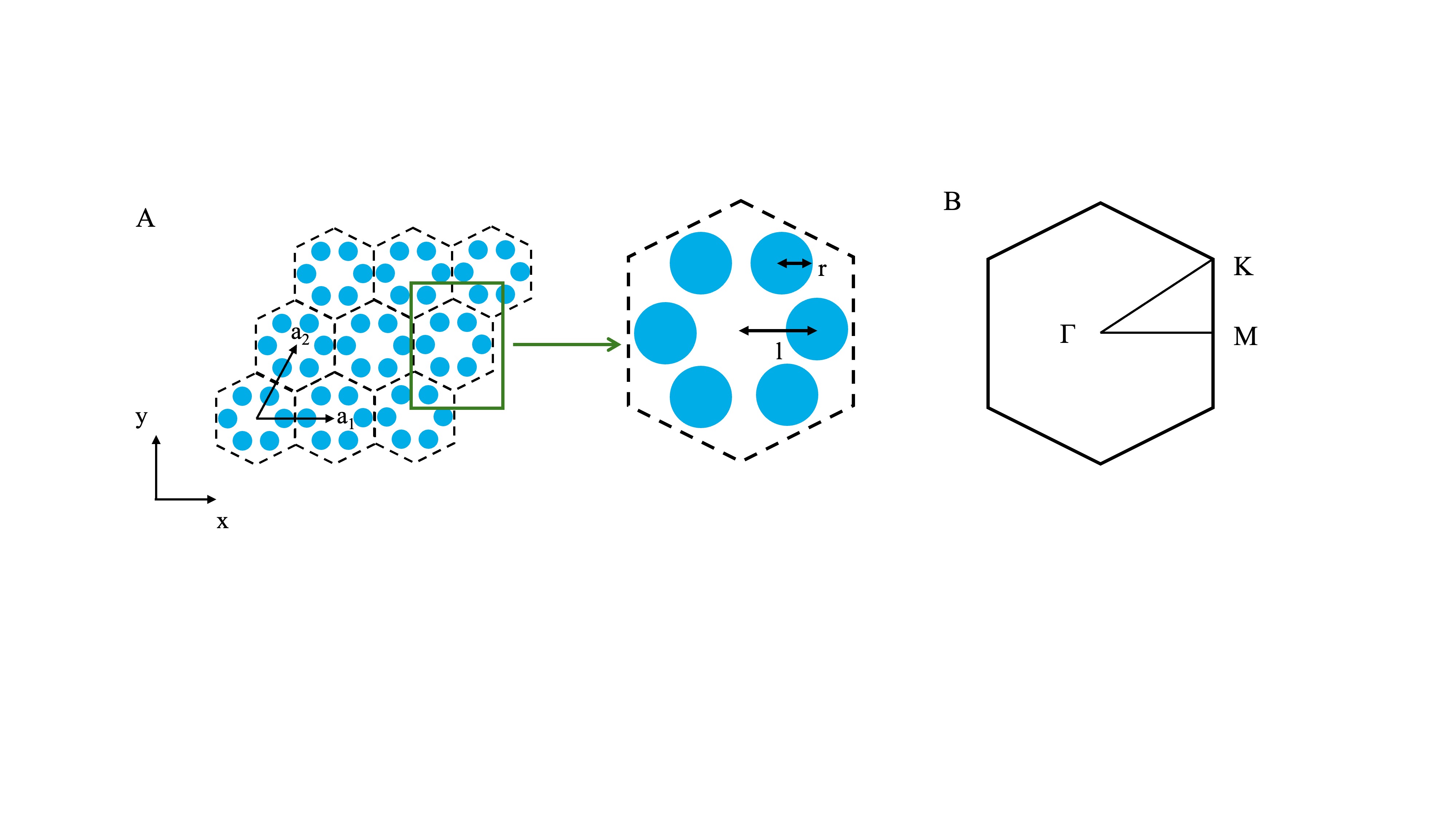
Figure 1 A. C6 symmetrical photonic crystal structure diagram, the right figure is the original cell of the photonic crystal (lattice constant is a=640nm, dielectric rod radius is r=65nm). B. A view of the first Brillouin zone of a honeycomb structure. The solid line representation is the path used for band calculation.
In these two kinds of photonic crystals, all the LN dielectric rods are aligned with the high symmetry direction of the hexagonal honeycomb lattice, which makes the whole crystal structure have C6v symmetry. According to the group theory, any eigenstate at the center of the Brillouin zone of these two crystals corresponds to the irreducible representation in the C6v point group, and there are two two-dimensional irreducible representations, which are called E1 and E2 irreducible representations. E1 indicates that the corresponding eigenstates have opposite parity for the mirror operations of the x-axis and y-axis, while E2 indicates that the corresponding eigenstates have the same parity for the mirror operations of the x-axis and y-axis, that is, E1 and E2 indicate that the corresponding eigenstates have odd parity and even parity symmetry under the spatial inversion operation. Based on these properties, we can change the photonic crystal from PC-I to PC-II by changing the center distance from the LN dielectric rods to the unit cell, to realize the transformation from topological trivial to topological nontrivial, that is, to achieve topological phase transition.
Subsequently, we solve the wave equation based on FEM, to obtain the eigenstates and corresponding band structures of photonic crystals. The three opposite sides of the hexagon are selected to set Floquet period conditions respectively, and the mesh setting is set as a conventional physical field control mesh. Figure 2A and Figure 2C show the band structures of PC-I and PC-II photonic crystals. It can be seen from the figure that PC-I and PC-II photonic crystals have two double degeneracies at Γ point. The electric field diagram is shown in Figure 2B and Figure 2D. Obviously, one pair of double degenerate states is two dipole states, and the other pair of double degenerate states is two quadrupole states. The dipole state and the quadrupole state appear together, and both have the same symmetry with the p and d orbitals in the electronic system. Therefore, the dipole state and the quadrupole state are called the p state and the d state respectively.
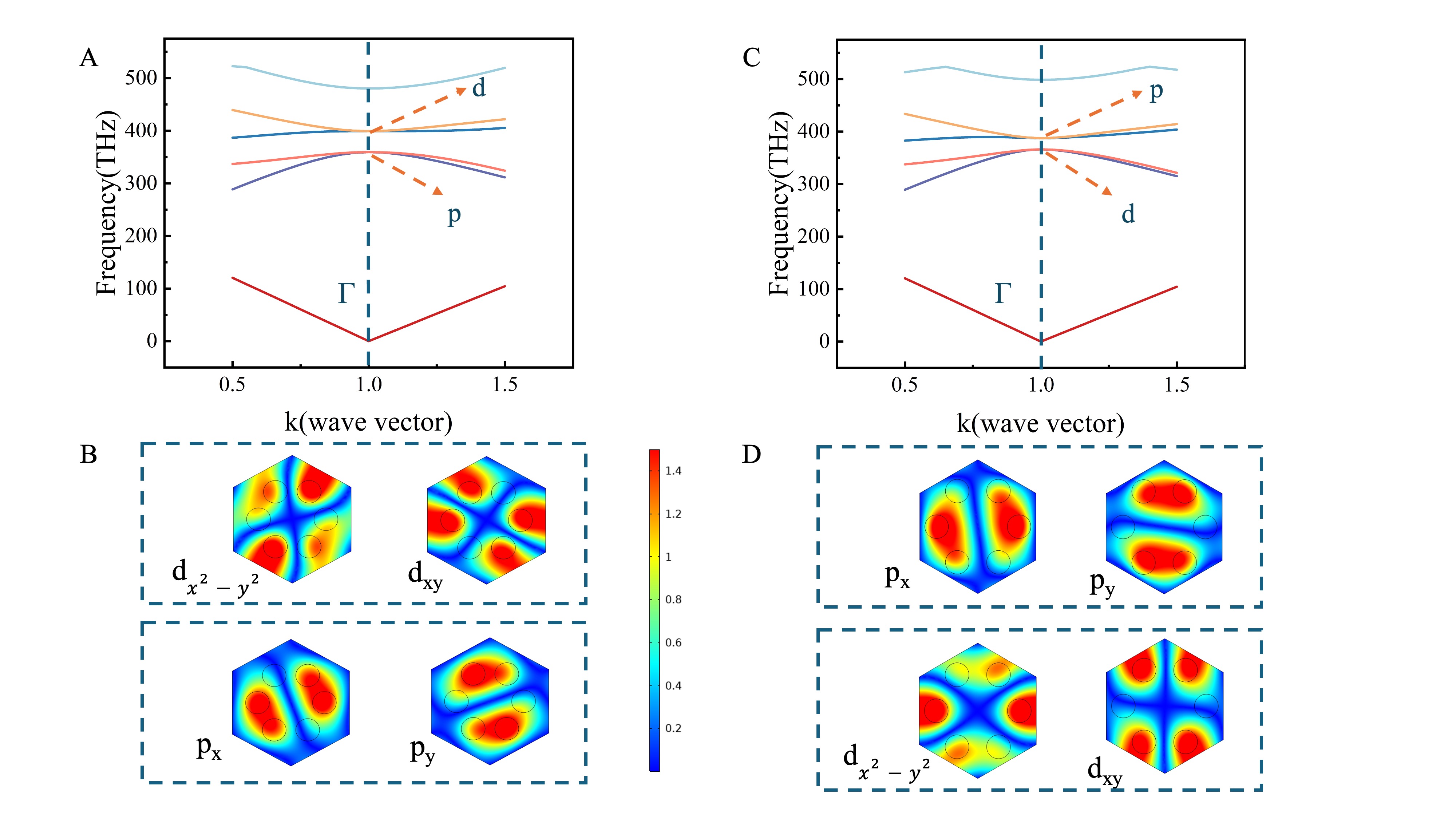
Figure 2 . The energy band diagram and intrinsic electric field diagram of LN photonic crystal with positive and negative band order. A. l<a/3 band diagram. B. l<a/3 intrinsic electric field diagram. C. l>a/3 band diagram. D. l> a/3 intrinsic electric field diagram.
As the previous analysis of the symmetry of photonic crystals, the p state is the state corresponding to the degenerate energy E1, and the d state is the state corresponding to the degenerate energy E2. The eigenstates with even-parity and odd-parity symmetry in the x-axis and y-axis of the p-state are denoted as the px state, and the other is denoted as the py state. The eigenstates with even parity symmetry for both x-axis and y-axis in the d-state are denoted as dx2-y2 state, and the other is denoted as dxy state. When l increases to $ l = \frac{a}{3} $, the double degenerate eigenenergy E1 of the p state at Γ is equal to the double degenerate eigenenergy E2 of the d state, and the double Dirac point of the quadruple degenerate state appears, as shown in Figure 3. When l continues to increase to $ l > \frac{a}{3} $, the double Dirac point at the Γ point disappears, the degeneracy occurs, and the double degeneracy occurs again.[33,34]
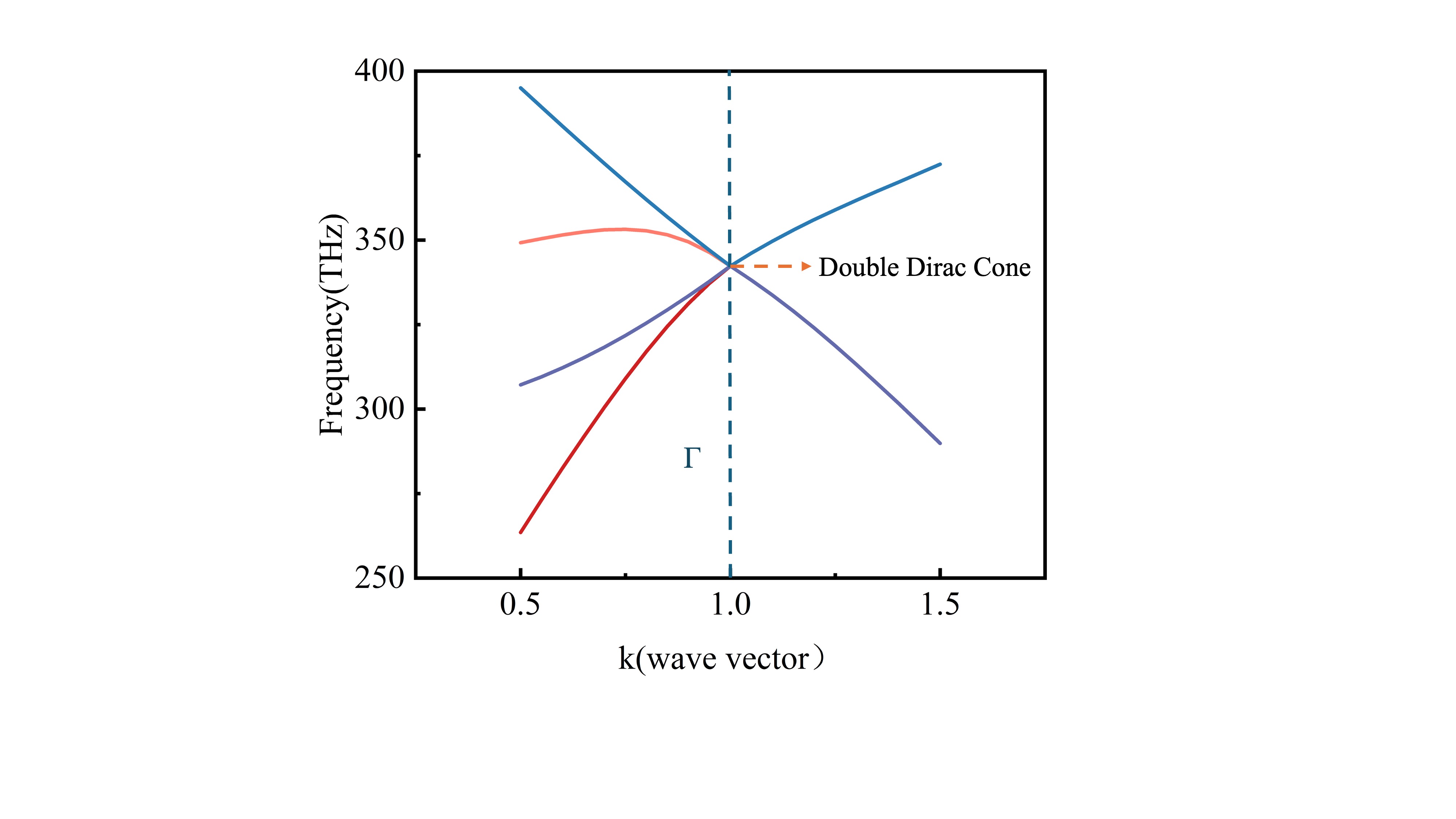
Figure 3 The band diagram of double Dirac points appears when p-band and b-band are closed.
To further understand the topological properties of the band gaps of the two crystals in Figure 2, the effective Hamiltonian near Γ point is obtained according to the perturbation theory, and the corresponding spin Chern number is calculated.[35-39] The k·p perturbation theory is to take the function $ \mu_{n}k_{0}$ and $ E_{n}\left( k_{0} \right)$ at the known $ k_{0}$ as the zero-order approximation, find $\mu$ and E at $k = k_{0} + \Delta k$, and gradually extend to the entire Brillouin zone through $\Delta k$. Based on the symmetry of the C6 point group of the structure, after complex calculations, the Hamiltonian near Γ point is given:
where $A = \frac{\left| \left\langle {x\left| \frac{\partial}{\partial} \right|x^{2} - y^{2}} \right\rangle \right|}{E_{1} - E_{3}}$, $B = \frac{\left| \left\langle {x\left| \frac{\partial}{\partial} \right|2xy} \right\rangle \right|}{E_{1} - E_{4}}$, the formula is the same as the result of the tight-binding model. On another set of ground state $\left\lbrack p_{x},p_{y},d_{x^{2} - y^{2}},d_{xy} \right\rbrack$, we obtain:
where $k_{\pm} = k_{x} \pm ik_{y}$, $G = \frac{A - B}{2},~~F = \frac{A + B}{2},{~k}_{1}^{2} = k_{x}^{2} + k_{y}^{2},~~k_{2}^{2} = k_{x}^{2} - k_{y}^{2}$, and A is a pure imaginary number. According to the effective Hamiltonian described by the equation, the photon system designed by us will have optical quantum spin Hall effect due to band inversion. To further verify this conclusion, it is necessary to calculate the spin Chern numbers corresponding to the two band gaps. The spin Chern number can be easily calculated by the following formula:
where $M = \frac{\omega_{d} - \omega_{p}}{2}$ is half the difference between the characteristic frequencies of the quadrupole mode (d-mode) and the dipole mode (p-mode) and N comes from the diagonal elements of the second-order pertur- bation term which is typically negative. For the PC-I type photonic crystal in Figure 2A, M>0, N<0, the result of spin Chern number is 0, which indicates that the corresponding band gap is topological trivial; for the PC-II type photonic crystal in Figure 2C, M<0, N<0, the result of the spin Chern number is $\pm 1$, so the corresponding band gap is topological nontrivial. By changing the distance from the dielectric rod to the center of the unit cell, we can realize the topological phase transition from the trivial state to the nontrivial state based on the band flipping.
3. Influence of Structural Parameters on Band Properties
To systematically investigate how structural parameters influence the energy band properties of LN photonic crystals, we examine three critical geometric parameters: the lattice constant a of the photonic crystal structure, the radius r of the dielectric rods, and the distance l between each dielectric rod and its unit cell center. These parameters directly influence both the photonic band structure and topological properties of the crystal. Throughout this study, we use LN (with refractive index n=1.99) as the dielectric rod material, while keeping air as the background medium. Our investigation proceeds as follows:
Firstly, the lattice constant a (a=640nm) and the radius of the dielectric rods r (r=65nm) are kept unchanged, and only the distance l from the dielectric rod to the center of the unit cell is changed. Therefore, the influence of the expansion of the hexagonal honeycomb structure in the LN photonic crystal cell structure on the photonic band and properties of the photonic crystal is explored. The range of l is from 183 nm to 243 nm, every 3 nm is calculated once, and the energy band diagrams of several representative are displayed as shown in Figure 4. It can be found that when the distance l from the dielectric rod of the topological photonic crystal to the center of the unit cell is changed, the energy band properties of the photonic crystal will change significantly, and the larger the dielectric rod deviates from l=a/3, the wider the band gap will be, but all l<a/3 photonic crystals have the same topological properties, which exhibit topological trivial properties. On the contrary, all l>a/3 photonic crystals also have the same topological properties, which exhibit topological nontrivial properties, as shown in Figure 5A.
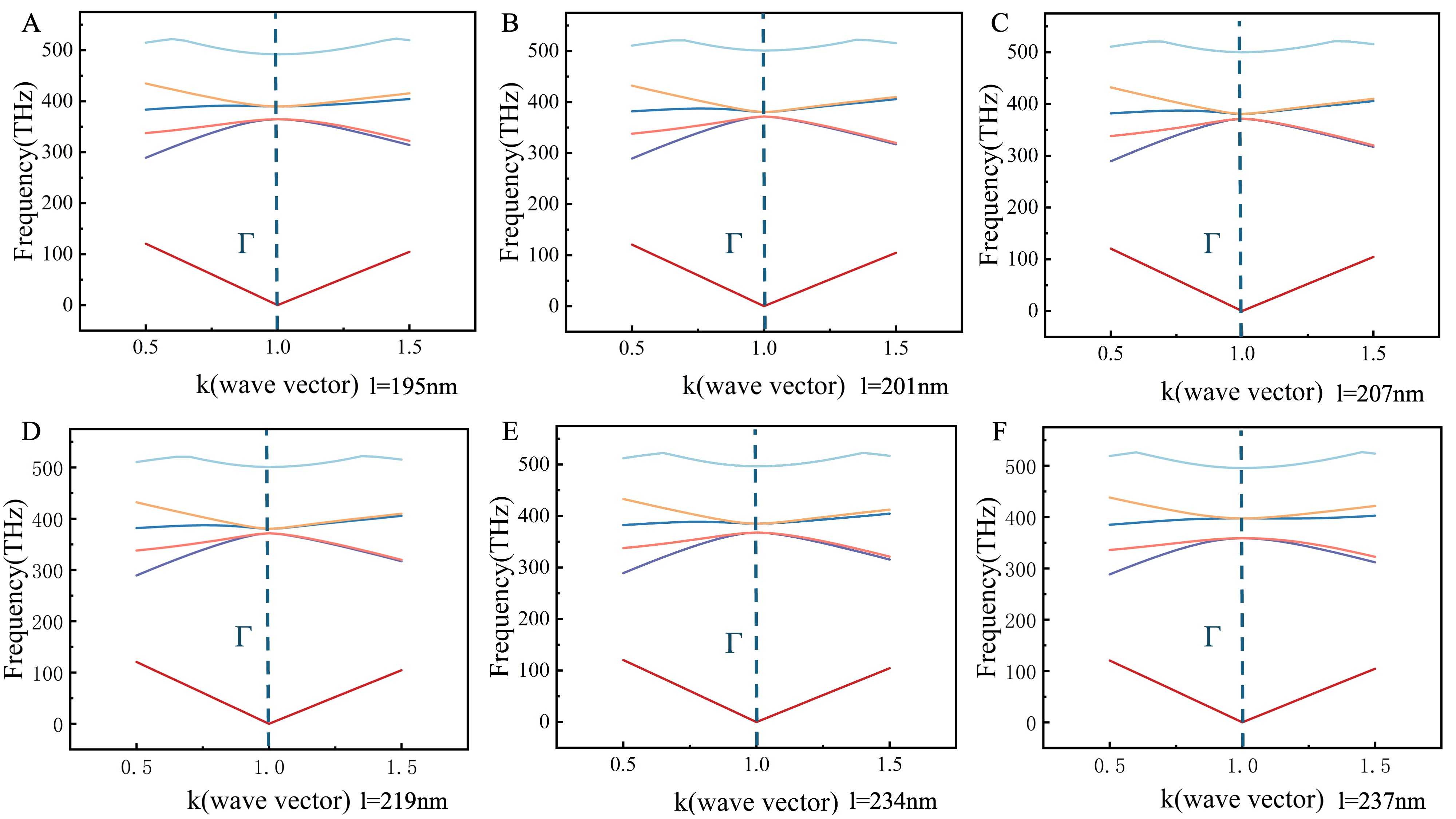
Figure 4 Energy band diagrams at different distances l
Secondly, when the distance between the dielectric rod and the center of the unit cell is fixed l=a/3, the radius r (r=65nm) and other parameters of the dielectric rod are kept unchanged, and only the lattice constant a of the photonic crystal cell is changed. The lattice constant a is taken from 200nm to 400nm, and calculated every 20nm. The characteristic frequency of the degenerate point under each lattice constant is shown in Figure 5B. It can be found that: in the position of the double Dirac point (l=a/3) with four-fold degeneration, without changing other parameters, only the lattice constant a of the photonic crystal is changed, the characteristic frequency of the degenerate point will gradually decrease with the increase of the lattice constant a. Then, other parameters such as the lattice constant a (a=640nm) of the photonic crystal structure are kept unchanged, and only the radius r of the dielectric rod is changed. The radius r is taken from 20 nm to 80 nm, and calculated every 10 nm. The characteristic frequency of the degenerate point at each radius is shown in Figure 5C. It can be found that: in the case of a four-fold degenerate double Dirac point position (l=a/3), without changing other parameters, only the radius of the photonic crystal dielectric rod is changed, the characteristic frequency of the degenerate point will gradually decrease as the radius r of the dielectric rod increases.
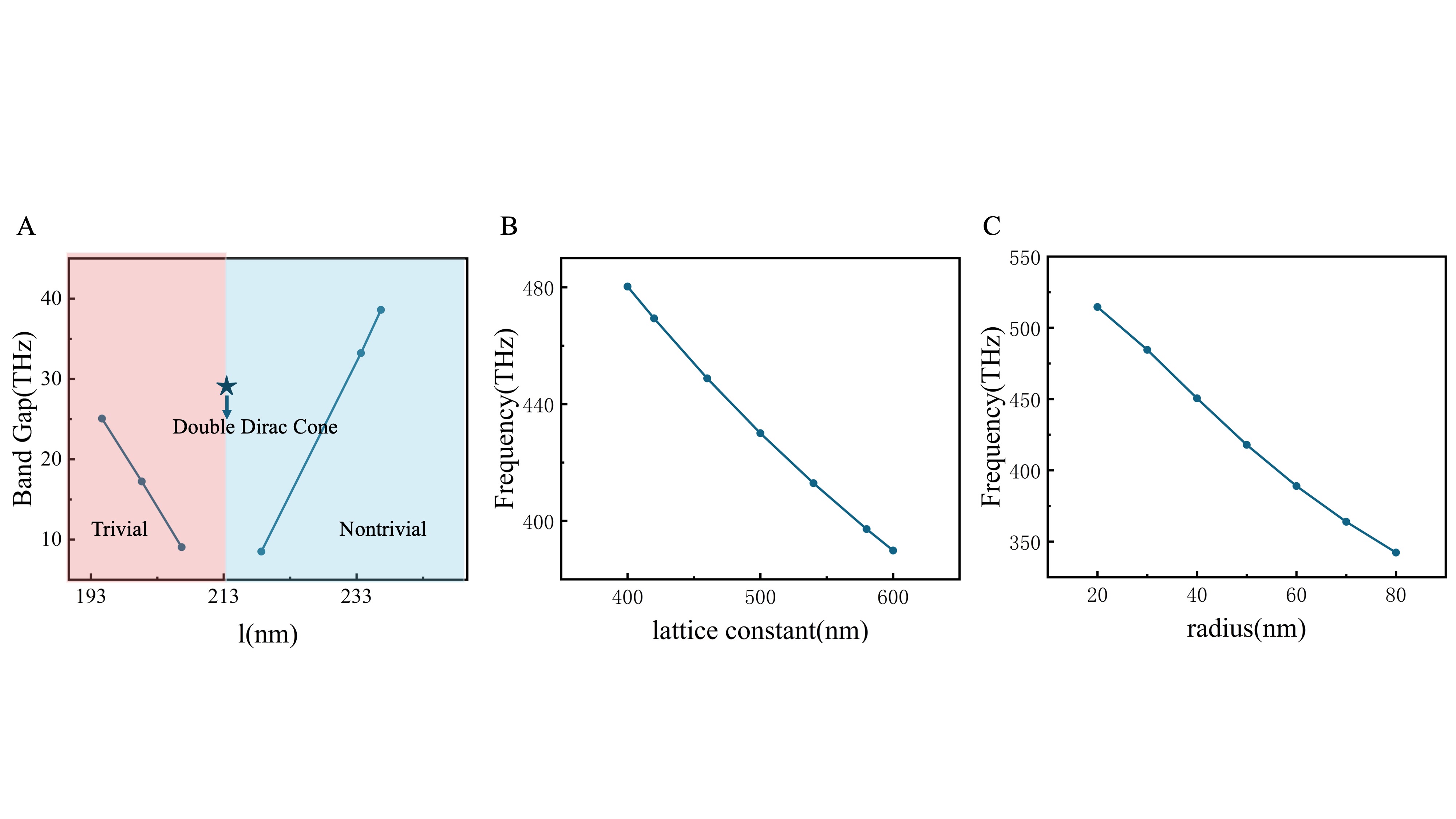
Figure 5 A. The variation of the photonic band gap with l. B. The variation of the characteristic frequency at the degenerate point with the lattice constant. C. The variation of the characteristic frequency at the degenerate point with the radius of the dielectric cylinder.
Synthesize the above discussion, it can be obtained that the band structure of the C6 symmetric topological photonic crystal based on LN has the following characteristics: when the distance from the dielectric rod to the center of the unit cell is l=a/3, a four-fold degenerate Dirac point will appear at the high symmetry point $\Gamma$. Here, the change of some parameters such as the lattice constant a and the radius r of the dielectric rod will not change the topological properties of the photonic crystal, but will only cause the photonic crystal band to move up and down. If the distance between the dielectric rod and the center of the original cell is not l=a/3, the quadruple degeneracy will be destroyed, and in a special position, the photonic crystal can appear two double degeneracy bands at the point $\Gamma$ and the forbidden band appears.
4. Topological Waveguide Design and Unidirectional Light Propagation
We designed a novel waveguide structure by combining two types of photonic crystals (PC-I and PC-II) with distinct topological properties. Each crystal type was arranged into a rectangular array of 26 × 12 unit cells, and these arrays were joined at inclination angles of 60° and 120° to create the waveguide interface. To investigate the waveguide's properties, we performed numerical simulations using three-point sources to generate circularly polarized light at the topological interface.
The simulation results demonstrate unique unidirectional propagation characteristics. When the phase of the three-point sources decreases counterclockwise, the system generates left-handed circularly polarized light, producing the electric field distribution shown in Figure 6A. This configuration excites left-handed chiral topological boundary states. Conversely, when the phase decreases clockwise, as illustrated in Figure 6B, the system generates right-handed circularly polarized light, exciting right-handed chiral topological boundary states.
Significantly, it was observed that light sources with identical frequencies but different phases, when placed at the same position along the interface, produced distinctly different propagation directions. This behavior was manifested as strictly unidirectional propagation: when the light source was positioned near the topological interface, the electromagnetic waves propagated exclusively leftward or rightward depending on their polarization state, demonstrating robust unidirectional propagation. At the same time, light propagation within the photonic bandgap frequency will be in a unidirectional. Optical transmission outside of the photonic band gap frequency will diffractional scatter in the plane of the photonic crystal.
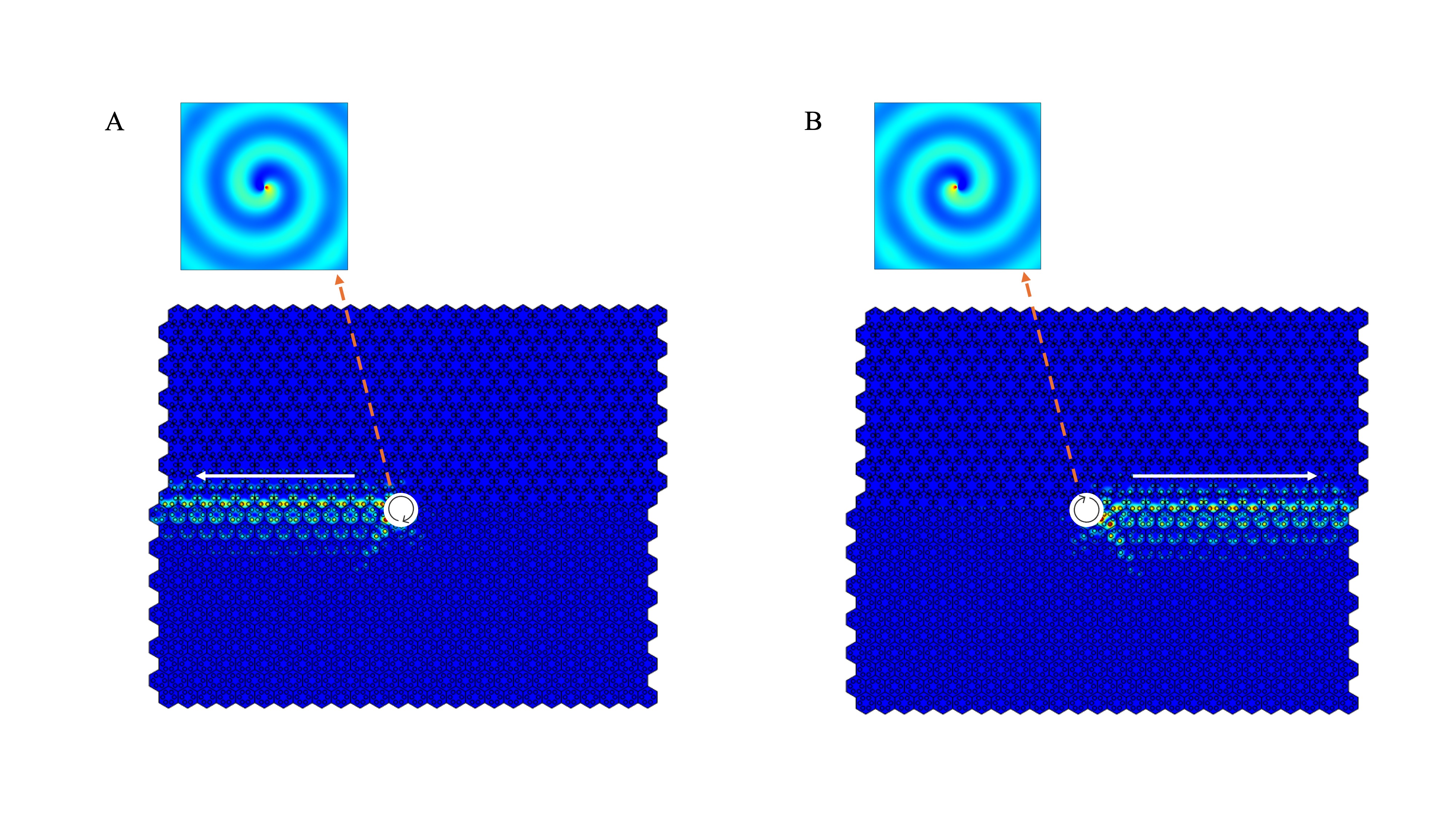
Figure 6 A. Unidirectional transmission of left-handed circularly polarized light. B. Unidirectional transmission of right-handed circularly polarized light.
The beam splitter serves as a critical component in integrated optical paths, enabling the separation of light fields into different paths with specific proportions. The splitting efficiency significantly influences the overall transmission efficiency of the integrated optical system. Correspondingly, the photonic crystal beam combiner functions to couple multiple light beams from different optical paths into a single beam.
A Y-shaped waveguide structure, functioning as both a beam splitter and combiner, was designed using LN dielectric rod photonic crystals. Numerical simulations demonstrated efficient beam splitting and combining capabilities, meeting the requirements for integrated optical path applications.
The detailed structure of the Y-shaped waveguide is illustrated in Figure 7. The beam splitter configuration, shown in Figure 7A, was constructed by splicing PC-I and PC-II photonic crystals at 60° and 120° tilt angles, integrated with a straight waveguide. The edge state analysis revealed that the structure effectively divides the incident light into two components and guides them along the corresponding boundaries, thus functioning as an optical beam splitter.
The beam combining functionality is demonstrated in Figure 7C, where the edge state transmission results are presented. When two separate light beams are introduced into the structure, they are effectively coupled into a single beam that propagates forward. The frequency range of operation can be controlled by adjusting three key parameters: the lattice constant, the LN dielectric rod dimensions, and the distance between the rod and the lattice center. These adjustable parameters make the Y-shaped photonic crystal waveguide particularly suitable for highly integrated optical systems.
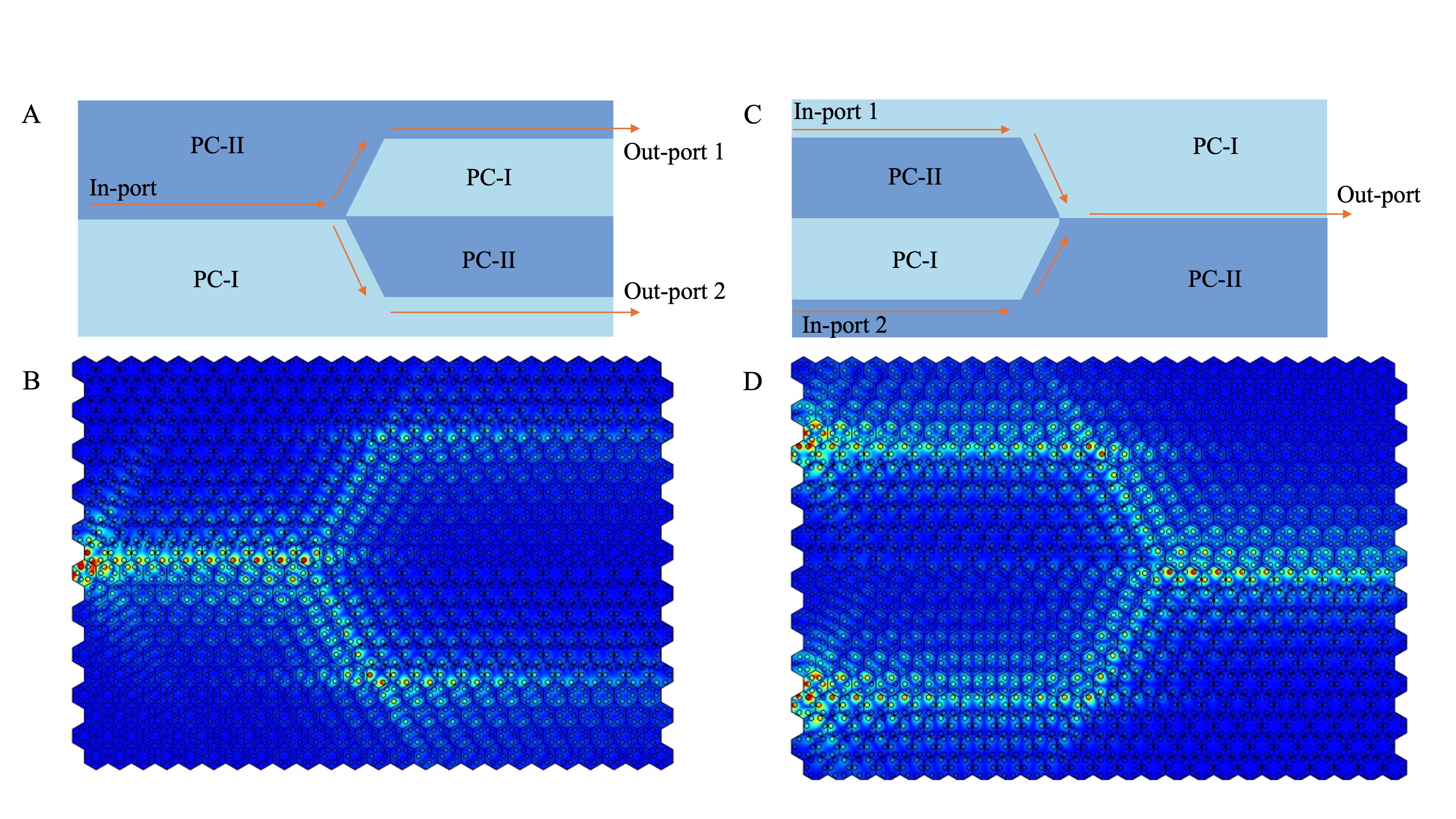
Figure 7 Edge states of Y-shaped photonic crystal waveguide.(Two kinds of photonic crystals with different topological phases are spliced together to merge or separate optical signals by using the unidirectional transmission boundary states at the interface) A. Geometric structure of LN photonic crystal beam splitter. B. electric field diagram of LN photonic crystal beam splitter. C. Geometric structure of LN photonic crystal combiner. D. electric field diagram of LN photonic crystal combiner.
Conclusion
A novel topological photonic crystal structure based on LN dielectric rods was designed and investigated. The structure demonstrated band inversion between double degenerate dipole and quadrupole modes, with the topological phase transition identified as the fundamental mechanism driving this band inversion. Through finite element method (FEM) simulations, the hexagonal honeycomb structure's geometric parameters were systematically analyzed, revealing the quantitative relationships between structural parameters (lattice constant a, rod radius r, and distance l) and the photonic band properties. Robust unidirectional light propagation was demonstrated at the interface between regions with different topological properties, with propagation direction controlled by the polarization state of the incident light. Furthermore, a Y-shaped waveguide structure incorporating these topological properties was designed and demonstrated to function effectively as both a beam splitter and combiner, showing high efficiency in beam manipulation. The simulation results revealed excellent performance in both beam splitting and combining operations, suggesting promising potential for applications in highly integrated optical systems. These findings provide practical insights for developing advanced topological photonic devices with controlled light propagation characteristics.
References
- He, L., Zhang, M., Shams-Ansari, A., Zhu, R., Wang, C., Marko, L. "Low-loss fiber-to-chip interface for lithium niobate photonic integrated circuits." Optics Letters. 2019, 44, 9, 2314-2317.
- Desiatov, B., Lončar, M., Holzgrafe, J., Zhang, M., Shao, L., Zhu, D., Sinclair, N., Yu, M., Reimer, C., Cheng, R., Shams-Ansari, A., Hu, Y., Puma, E., Ghosh, S., Xin, C. J. "Integrated photonics on thin-film lithium niobate." Optics. 2021, 13, 242-352.
- Chen, G., Li, N., Ng, J. D., Lin, H.-, Zhou, Y., Fu, Y. H., Lee, L. Y. T., Yu, , Liu, A.-Q., Danner, A. J.. "Advances in lithium niobate photonics: development status and perspectives." Advanced Photonics. 2022, 4, 3.
- Minakata, M. "LiNbO3 optical waveguide devices." Electronics and Communications in Japan (Part II: Electronics). 1994, 77, 11, 37-51.
- Bazzan, M., Sada, C. "Optical waveguides in lithium niobate: Recent developments and applications." Applied Physics Reviews. 2015, 2, 4, 040603.
- Zhou, J., Liang, Y., Liu, Z., Chu, W., Zhang, H., Yin, D., Fang, Z., Wu, R., Zhang, J., Chen, W., "On-chip integrated waveguide amplifiers on Erbium-doped thin film lithium niobate on insulator." Laser & photonics reviews. 2021, 15, 8, 2100030.1-2100030.7.
- He, R., An, Q., Jia, Y., Castillo-Vega, G. R. "Femtosecond laser micromachining of lithium niobate depressed cladding waveguides." Optical Materials Express. 2013, 3, 9, 1378-1384.
- Jia, Y., Wu, J., Sun, X., Yan, X., Xie, R., Wang, L., Chen, Y., Chen, F. "Integrated Photonics Based on Rare-Earth Ion-Doped Thin-Film Lithium Niobate." Laser & Photonics Reviews. 2022, 16, 9, 2200059.
- Li, G., Jia, Y.-C., Chen, F. "Research progress of photonics devices on lithium-niobate-on-insulator thin films." Acta Physica Sinica. 2020, 69, 15.
- Wu, L.-H., Hu, X. "Scheme for Achieving a Topological Photonic Crystal by Using Dielectric Material." Physical Review Letters. 2015, 114, 22.
- Wang, H., Gupta, S. K., Xie, B., Lu, M. "Topological photonic crystals: a review." Frontiers of Optoelectronics. 2020, 13, 1, 50-72.
- Sun, H., Yang, B., Yu, W., Hu, Z.-D., Wu, J., Zhu, Y., Wang, J., Yang, Y. "Observation of multifunctional robust topological states based on asymmetric C4 photonic crystals." APL Photonics. 2024, 9, 10.
- Wang, L., Jian, S. K., Yao, H. "Topological photonic crystal with equifrequency Weyl points." Physical Review A. 2016, 93, 6, 061801.
- Alam, B., Ferraro, A., Caputo, R., Asquini, R. "Optical properties and far field radiation of periodic nanostructures fed by an optical waveguide for applications in fluorescence and Raman scattering." Optical and Quantum Electronics. 2022, 54, 307.
- Büttiker, M. "Absence of backscattering in the quantum Hall effect in multiprobe conductors." Physical Review B. 1988, 38, 14, 9375–9389.
- Calafiore, G., Cabrini, S., Penzo, E., Luca, A. C. D., Romano, S., Mocella, V., Zito, G. "Quantum Spin-Hall Effect of Light at Bound States in the Continuum." Optics. 2017.
- Wang, Z., Chong, Y., Joannopoulos, J. D., Soljačić, M. "Observation of unidirectional backscattering-immune topological electromagnetic states." Nature. 2009, 461, 7265, 772–775.
- Liu, W., Wu, C., Jia, Y., Jia, S., Chen, G., Chen, F. "Observation of edge-to-edge topological transport in a photonic lattice." Physical Review A. 2022, 105, 6, L061502.
- Huang, L., He, L., Zhang, W., Zhang, H., Liu, D., Feng, X., Liu, F., Cui, K., Huang, Y., Zhang, W., Zhang, X. "Hyperbolic photonic topological insulators." Nature Communications. 2024, 15, 1, 1647–1647.
- Jia, Y., Chen, F., Wang, L. "Ion-cut lithium niobate on insulator technology: Recent advances and perspectives." Applied Physics Reviews. 2021, 8, 1, 011307.
- Dong, J.-W., He, X.-T., Zhao, F.-L., Chen, X.-D., Yuan, J.-J., Qiu, H.-Y., Liang, E.-T. "A silicon-on-insulator slab for topological valley transport." Nature Communications. 2019, 10, 1, 872.
- Yatsugi, K., Funayama, K., Pandarakone, S. E., Matsui, T., Iizuka, H. "Square-root topological insulator for a dual-band photonic waveguide." Physics Letters A. 2024, 521, 129755–129755.
- Leykam, D., Chong, Y. D. "Edge Solitons in Nonlinear-Photonic Topological Insulators." Physical Review Letters. 2016, 117, 14, 143901–143901.
- Qi, X.-L., Zhang, S.-C. "Topological insulators and superconductors." Reviews of Modern Physics. 2011, 83, 4, 1057–1110.
- Hasan, M. Z., Kane, C. L. "Colloquium: Topological insulators." Reviews of Modern Physics. 2010, 82, 4, 3045–3067.
- Chen, M. L., jun Jiang, L., Lan, Z., Wei, E. I. "Pseudospin-polarized topological line defects in dielectric photonic crystals." IEEE Transactions on Antennas and Propagation. 2019, 68, 1, 609-613.
- Yang, P., Jiang, P., Guo, X., Hou, L. "Topologically protected Mach–Zehnder interferometer." Journal of Optics. 2020, 22, 10, 105001.
- He, X.-T., Li, M.-Y., Qiu, H.-Y., Ruan, W.-S., Zhou, L.-D., Liu, L., Chen, X.-D., Chen, W.-J., Zhao, F.-L., Dong, J.-W. "In-plane excitation of a topological nanophotonic corner state at telecom wavelengths in a cross-coupled cavity." Photonics Research. 2021, 9, 8, 1423–1431.
- Yang, Q., Yu, M., Chen, Z., Ai, S., Kentsch, U., Zhou, S., Jia, Y., Chen, F., Liu, H. "A novel approach towards robust construction of physical colors on lithium niobate crystal." Opto-Electronic Advances. 2025, 240193–1.
- Yan, B., Xie, J., Liu, E., Peng, Y., Ge, R., Liu, J., Wen, S. "Topological edge state in the two-dimensional Stampfli-triangle photonic crystals." Physical Review Applied. 2019, 12, 4, 044004.
- Noh, J., Huang, S., Chen, K. P., Rechtsman, M. C. "Observation of photonic topological valley Hall edge states." Physical review letters. 2018, 120, 6.
- Lu, L., Joannopoulos, J. D., Soljačić, M. "Topological photonics." Nature photonics. 2014, 8, 11, 821-829.
- Li, Y., Wu, Y., Chen, X., Mei, J. "Selection rule for Dirac-like points in two-dimensional dielectric photonic crystals." Optics Express. 2013, 21, 6, 7699–7711.
- Mei, J., Wu, Y., Chan, C. T., Zhang, Z.-Q. "First-principles study of Dirac and Dirac-like cones in phononic and photonic crystals." Physical Review B. 2012, 86, 3, 035141.
- Sheng, L., Li, H.-C., Yang, Y.-Y., Sheng, D.-N., Xing, D.-Y. "Spin Chern numbers and time-reversal-symmetry-broken quantum spin Hall effect." Chinese Physics B. 2013, 22, 6, 067201.
- Skirlo, S. A., Lu, L., Soljačić, M. "Multimode One-Way Waveguides of Large Chern Numbers." Physical Review Letters. 2014, 113, 11, 113904.
- Hatsugai, Y. "Chern number and edge states in the integer quantum Hall effect." Physical review letters. 1993, 71, 22, 3697.
- Sheng, D. N., Weng, Z. Y., Sheng, L., Haldane, F. D. M. "Quantum spin-Hall effect and topologically invariant Chern numbers." Physical review letters. 2006, 97, 3, 036808.
- Prodan, E. "Robustness of the spin-Chern number." Physical Review B—Condensed Matter and Materials Physics. 2009, 80, 12, 125327.