Femtosecond Laser Direct-written Type I Waveguides in LiTaO3 crystal
published: 26 April 2025 | https://doi.org/10.63174/xdi.OUYM9272
Abstract
This work employs Type I single-line and multi-line optical waveguides in LiTaO3 crystals by femtosecond laser direct writing. Investigating the critical factors influencing the success of high-performance waveguide fabrication. By systematically varying pulse energy, scanning speed, and focal depth, the effects of femtosecond laser direct writing modifications in LiTaO3 crystals were investigated, achieving a low insertion loss of 1.39 dB at a writing speed of 4 mm/s and a pulse energy of 0.42 μJ. Through multi- scan technique, three sets of multi-line optical waveguides with varying track spacings under parallel and perpendicular polarization orientations were fabricated. By tailoring the waveguide cross-sections into square or circularly symmetric profiles via scanning parameter optimization, precise control over modal distribution was achieved, enabling efficient guided-mode propagation at 1550 nm with minimized scattering losses. This work provides a straightforward and versatile approach for fabricating complex optical waveguide devices, enabling their applications in on-chip quantum information processing with enhanced integration flexibility.
1. Introduction
With the development of ultrafast laser technology, the femtosecond laser micro/nano machining technology experienced rapid development during the 1990s,[1] providing a flexible and highly efficient approach for fabricating components in integrated optics.[2-5] The development of fiber chirped pulse amplifiers (FCPA) in the early 21st century significantly advanced the application of femtosecond laser micro/nano machining technology,[6] Femtosecond laser micro/nano machining technology began to be applied to surface micromachining,[7] nanoablation,[8] internal modification within transparent materials,[9] as well as biomedical and industrial sectors.[10] In particular, the optical waveguides fabricated in transparent materials via femtosecond lasers serve as critical platforms for photonic quantum chips, enabling the realization of three-dimensional quantum random walks [11,12] and emerging as a pivotal technique for processing 3D quantum chips.[13,14] Based on the extent of lattice damage induced by femtosecond laser processing in transparent materials, the refractive index modifications are categorized into two distinct types:[15]Femtosecond laser irradiation can induce two types of modifications in the irradiated region: Type I modification with increased refractive index (Δn > 0) and Type II modification with decreased refractive index (Δn < 0). For Type I modification, the laser-written zone directly serves as the waveguiding region for light confinement. This phenomenon primarily occurs in amorphous glass and exhibits strong polarization dependence. Since the waveguide region coincides with the writing trajectory, the crystalline properties of the material in the modified zone are significantly disrupted. However, Type I waveguides offer the advantages of a simple structure and ease of direct writing, making them highly suitable for the fabrication of quantum chips or three-dimensional photonic devices. Type II modification induces an increase in refractive index in the surrounding regions of the inscribed tracks, forming the waveguiding core.[16] This type of modification is applicable to a wide range of crystalline materials, and the fabricated waveguides can preserve the intrinsic optical properties of the crystal. However, the fabrication time for Type II modification is significantly longer compared to Type I.[17] Therefore, optimizing the performance of Type I refractive index modification optical waveguides through key parameters such as waveguide cross-sectional geometry and refractive index profiles is critical for advancing the fabrication of quantum photonic integrated circuits and 3D photonic devices.
Lithium tantalate (LiTaO3) crystal is a versatile transparent crystalline material belonging to the same family as lithium niobate (LiNbO3) crystal,[18] which exhibits superior properties including electro-optic, acousto-optic, piezoelectric, pyroelectric, photorefractive, and nonlinear optical characteristics, enabling its widespread applications in high-frequency surface acoustic wave (SAW) filters, optical resonant filters, high-performance pyroelectric infrared detectors, optical parametric oscillators, and related photonic devices.[19-22] The LiTaO3 crystal belongs to the trigonal crystal system with three-fold rotational symmetry, crystallizing in an ilmenite-type ABO₃ lattice structure. It exhibits a paraelectric phase above the Curie temperature and transitions to a ferroelectric phase below the Curie temperature, demonstrating superior pyroelectric effects. The LiTaO3 crystal exhibits unique advantages in certain optical properties, such as a shorter ultraviolet absorption edge, enhanced resistance to optical damage, and lower coercive fields. Consequently, optical waveguide devices based on LiTaO3 crystals have emerged as a focal point of research.[23-25]
In this paper, by altering the writing parameters of the femtosecond laser, the influence on the morphology of femtosecond laser-induced traces is investigated, the transition from Type I refractive index increase modification to Type II refractive index decrease modification has been achieved. In the end, single-line and multi-line optical waveguides with Type I refractive index increase were successfully created in LiTaO3 crystals through femtosecond laser direct writing. Single-line optical waveguides with different writing speeds and different pulse energies were characterized through 633 nm end-face coupling experiments, multi-line optical waveguides under different polarization conditions were characterized through 633 nm and 1550 nm end-face coupling experiments. The optical waveguide fabricated based on Type I refractive index modification may be helpful for the quantum chip information.
2. Experiment
2.1. Preparation of Type Ⅰ refractive index increased single-line and multi-line optical waveguides
In this work, we use a LiTaO3 crystal with the dimension of 10 × 10 × 1 mm3, both end faces and both large faces of the crystal are optically polished. The femtosecond laser system used for waveguide fabrication is a yttterbium fiber femtosecond laser system (Origami-10 XP, OneFive, Swizerland), which is operating at a central wavelength of 1031 nm, pulse width of 420 fs, repetition rate can be adjusted between 1 kHz and 1 MHz. During the process, the sample is placed on a three-axis (XYZ) motorized stage, with a resolution of 100 nm in the horizontal direction and 1 µm in the vertical direction. Through a preset program, the three-dimensional movement direction and scanning speed of the sample are controlled. The femtosecond laser beam is focused beneath the surface of the sample by a 40 × microscope objective with numerical aperture (N.A.) of 0.6, the CCD is installed above the microscope objective, through fiber optic lighting system, the scanning direction is strictly parallel to the long axis (y-axis, 10 mm) of the sample and monitor the femtosecond laser direct writing process in real time. In the experiment, a combination of a motorized half-wave plate and a polarizer is employed to continuously adjust the laser writing pulse energy, while neutral density (ND) filters could be incorporated to further extend the adjustment range. Glan-Taylor prisms and polarizers are used to control the polarization direction, combined with a motorized shutter to precisely regulate the pulse triggering timing, thereby enabling the fabrication of complex structures.
Single-line optical waveguides are prepared by fixing the pulse energy at 0.71 J and employing different scanning rates (2-5 mm/s), the optimal scanning rate of 4 mm/s is selected, and the laser pulse energy is systematically varied in a continuous manner, by employing different direct-writing laser pulse energies of 0.38 µJ, 0.42 µJ, 0.71 µJ, 0.94 µJ, 1.16 µJ and 1.35 µJ, six optical waveguides are prepared.
For multi-line optical waveguides, the scanning rate and pulse energy are selected as 4mm/s and 0.89 µJ, respectively. A multiple scanning technique is employed to spatially arrange parallel written tracks, forming a square-shaped symmetric region with elevated refractive index, thereby confining the waveguide core within this area. Multi-line optical waveguides are fabricated with varying laser polarization directions (parallel and perpendicular), spacing intervals (1µm, 2µm and 3µm), and corresponding numbers of written tracks.
2.2. The test of waveguides characterization
The end facet morphology of the waveguide structures is imaged using a metallographic microscope. Based on an end-face coupling system, a He-Ne laser with an output wavelength of 632.8 nm is employed as the probe light source, the polarization direction is adjusted by rotating the half-wave plate, the laser is vertically coupled into the crystal end facet by a 25 × incident objective with numerical aperture (N. A.) of 0.4, the output laser is collected by an another identical objective, the near-field mode distribution and output power of the waveguide are measured using a CCD and a power meter, respectively. Furthermore, a 4-λ fiber laser with 1550 nm is employed as the probing light source, a mid-infrared (MIR) objective lens and an MIR-optimized CCD camera coupled to acquire the emitted laser characteristics.
3. Results and discussion
3.1. The influencing factors of waveguides preparation
3.1.1. Pulse energy
Under a fixed scanning speed of 4 mm/s, the influence of pulse energy of 0.48 µJ, 0.50 µJ, 0.53 µJ, 0.74 µJ, 0.85 µJ, and 1.06 µJ on the writing of traces is investigated, two scanning passes are performed at the same pulse energy with an inter-track spacing of 20 μm. At pulse energies of 0.47 μJ and 0.50 μJ, transparent area (waveguide area) was observed. When the pulse energy increased to 0.53 μJ, a stretched black filamentous modification zone began to emerge within the transparent areas, As the pulse energy increases, the length of the written traces increases from 12.77 μm to 44.17 μm, the transparent area (waveguide area) gradually moves down, and a stretched black filamentous modification zone appears at the front end of the laser beam. The analysis reveals that when the laser energy exceeds a critical threshold, nonlinear mechanisms in the material (Kerr effect) are initiated. The competition between laser self-focusing and plasma defocusing dynamically extends the focal depth of the laser beam, thereby lengthening the optical filamentation region.[26,27] In the LiTaO3 crystal, the critical threshold for self-focusing is:[25]
Where n0 = 2.18, n2 = 0.91×10⁻¹⁵ cm2 W-1, therefore, Pcr =0.80 MW,[28] the corresponding pulse energy is 0.38 µJ. When the laser power P = 1.4Pcr, nonlinear self-focusing occurs, leading to elongation of the ablation mark length.
3.1.2. Scanning speed
Under a fixed pulse energy of 0.49 µJ, the influence of scanning speed of 1 mm/s, 2 mm/s, 3mm/s, 4mm/s, 5mm/s, and 6mm/s on the writing of traces was investigated, two scanning passes are performed at the same scanning speed with an inter-track spacing of 20 μm. Because the pulse energy is below the self-focusing threshold, the length of the written traces are virtually no change. At a scanning speed of 6 mm/s, transparent area (waveguide area) was observed. When the scanning speed was reduced to 3 mm/s, black filamentous modification zone began to emerge within the transparent areas. As the scanning speed further slows down, the writing of traces gradually changes from Type I transparent refractive index modification to Type II black refractive index damage, because the temporal and spatial overlap between consecutive pulses in the writing unit becomes more pronounced with reduced scanning speed. This exacerbates the energy flux density at the focal spot core, thereby inducing lattice damage, so it will evolve from a smooth and uniform refractive index increase modified area to a lattice damage area with a reduced refractive index.
3.1.3. Focusing depth
Figure 1 A investigates the effect of varying the depth of focus (30-700 μm, trace spacing of 40 μm ) on the writing of traces, the pulse energy of 20 J and the scanning speed of 4mm/s is selected. Figure 1 B presents the dependence of writing traces length on the depth of focus, categorized into three characteristic phases based on the observed behavior, in Region I (near-surface region, 30-200 μm), spherical aberration induced by surface refraction results in longitudinal elongation of the focal region, leading to an increase in trace length with increasing depth of focus. In Region Ⅱ (250-350 μm), with the increase in depth of focus, the length of the written traces has decreased and black “dot-like” structures have emerged, this is because the optical Kerr effect enables sufficient transmission distance to be achieved, promoting self-focusing of the laser beam itself, resulting in the “black spot” storing part of the laser energy. In Region Ⅲ (380-700 μm), long-distance transmission causes the laser energy to linearly attenuate, resulting in the inability to effectively confine the focused area. Consequently, the trace length becomes shorter and less clear. The processing is typically conducted in the near-surface region, and the fabrication of optical waveguides in this work utilized a focal depth of 150 μm.
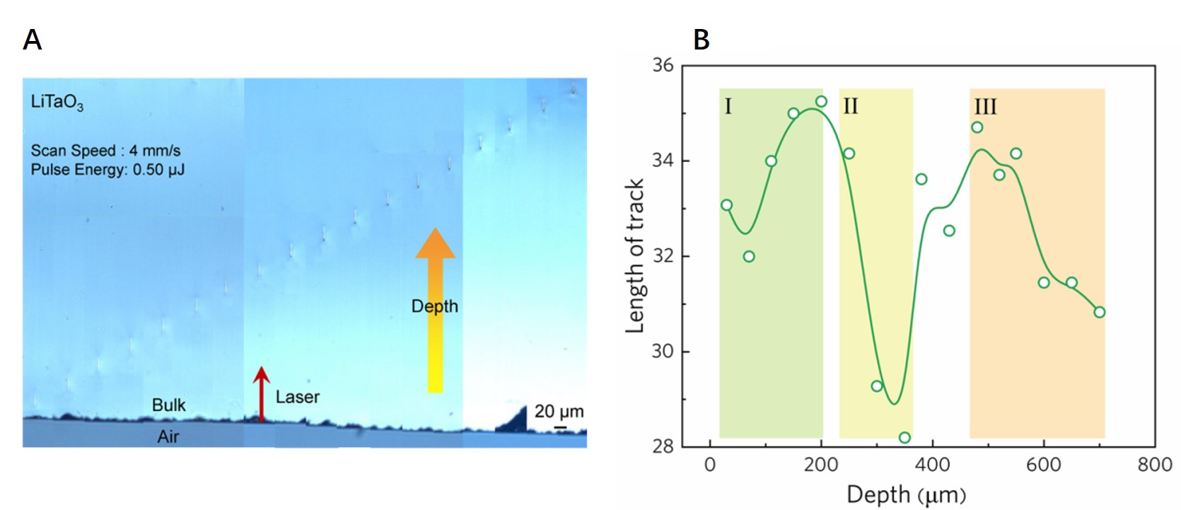
Figure 1 A Microscopy image of LiTaO3 crystal traces at different laser scanning rates. B Variation in the length of writing traces in LiTaO3 crystals with focus depth.
3.2. Type I refractive-index-enhanced single-line optical waveguides
An end-face coupling system was implemented to characterize single-mode optical waveguides with varying scanning velocities. The characterization protocol employed a He-Ne laser source emitting at 632.8 nm, with polarization orientation controlled via a half-wave plate. Beam coupling was achieved through a 25×objective lens, followed by signal collection using the same objective. Near-field mode profiles and output power were simultaneously monitored through a CCD camera and optical power meter, respectively. Figure 2 presents microscopy images of single-line optical waveguides fabricated in the LiTaO3 crystal at different scanning speed, along with their near-field mode distribution profiles under 633 nm. With the increase of scanning speed, the length of the traces gradually shortens, this waveguide exclusively supports the guided mode propagation in the TM mode, which aligns with the transmission characteristics of Type I single-line optical waveguides in other crystals.
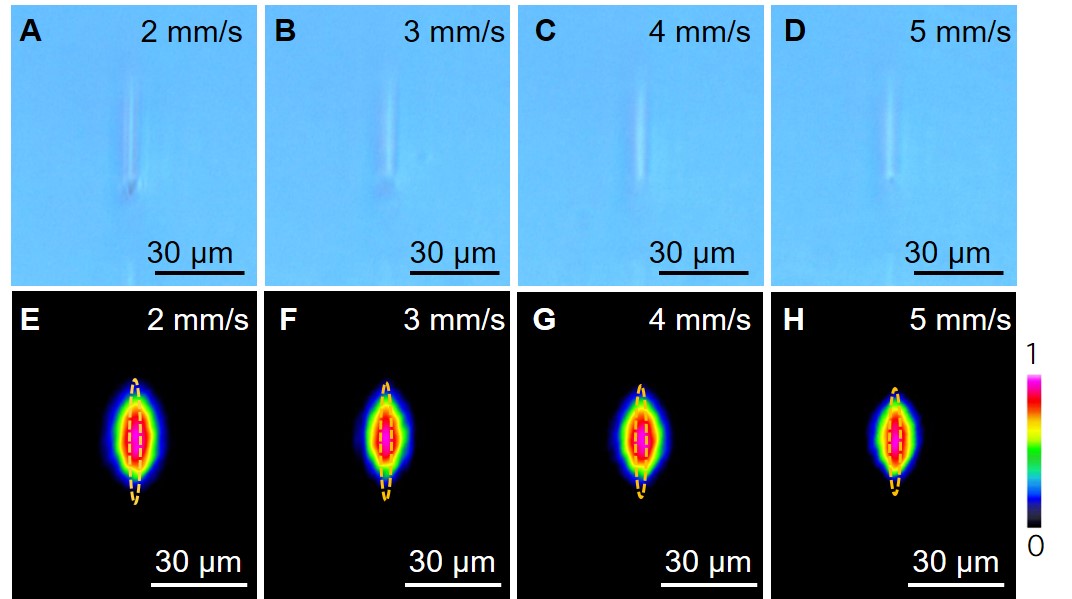
Figure 2 A-D Microscope images of single-line optical waveguides in the LiTaO3 crystal at different writing speeds under a pulse energy of 0.71 μJ; E-H The near-field mode distribution of the corresponding waveguide at 633 nm.
Figure 3 presents microscopy images of single-line optical waveguides at different pulse energy, along with their near-field mode distribution profiles. As the pulse energy increases, the length of the written traces grow, and the mode distribution gradually elongates longitudinally along the laser writing direction, the transmission evolves from the TM00 fundamental mode to multimode propagation. At a writing speed of 4 mm/s, the calculated results indicate that the lowest insertion loss of 1.39 dB is achieved at an energy of 0.42 J.
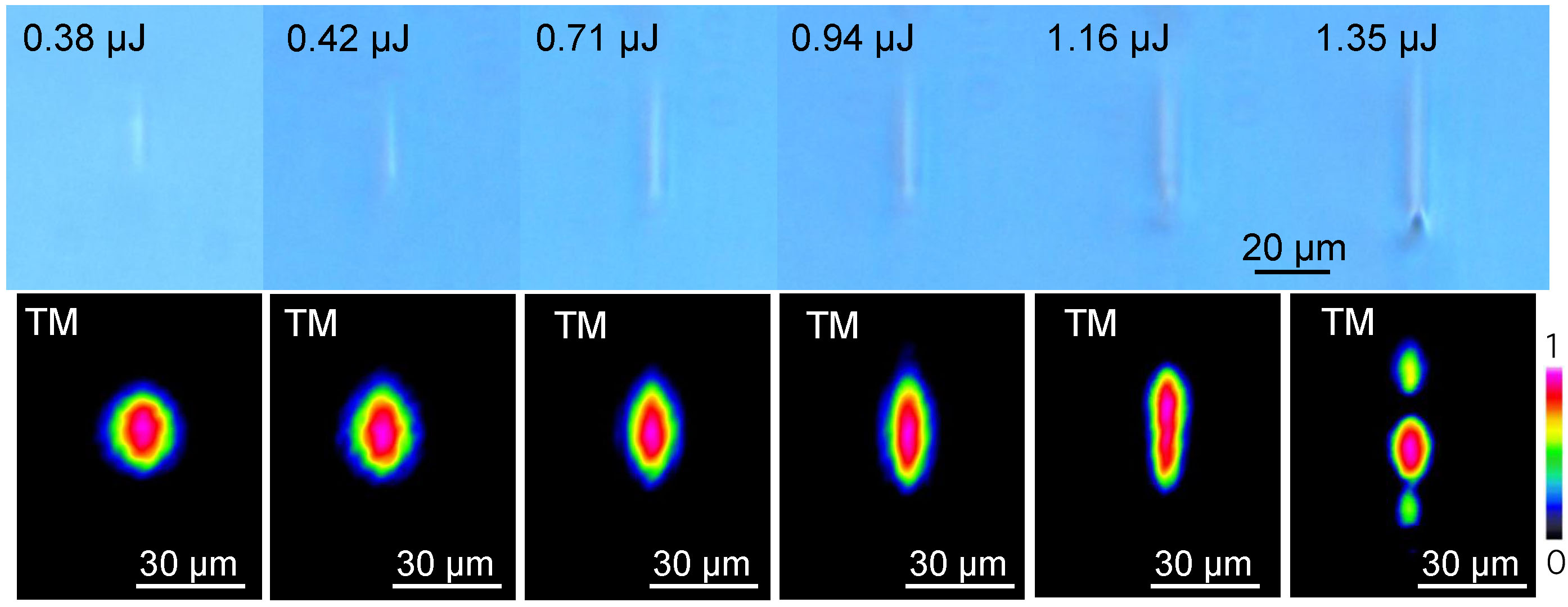
Figure 3 Microscope images of single-line optical waveguides in the LiTaO3 crystal at different pulse energy under a scanning speed of 0.71 μJ and the near-field mode distribution.
3.3. Type I refractive-index-enhanced multi-line optical waveguides
In the application of waveguide devices, it is typically demanded that the modal distribution of the cross-section should be of circular symmetry type. For single-line optical waveguides, the distribution takes the form of a narrow and elongated ellipsoid. The multi-mode optical waveguide is capable of supporting symmetrical and scalable modal distributions.
We fabricated multi-line optical waveguides by using multiple scanning techniques. The multiple scanning techniques can accumulate heat, causing densification of the material and thereby increasing the refractive index. The multiple scanning can also improve the geometric symmetry of the waveguides and reduce birefringence. Compared to single-line optical waveguides, multi-line fabricated optical waveguides achieve enhanced performance through tailored cross-sectional geometry and refractive index profiles. Among them, the scanning interval and the number of scans affect the refractive index and geometric symmetry of the optical waveguides fabricated by the multiple scanning techniques. We fabricated three groups of multi-line optical waveguides under different polarizations by changing the scanning interval and the number of scans. Figure 4 shows microscope images of three sets of multi-line optical waveguides fabricated with different trace intervals and scanning passes under parallel polarization. The intervals between traces No.1-No.3 are 1 μm, No.4-No.11 are 2 μm, No.12-No.14 are 3 μm, among them, No.8 has an end-face dimension of 31.16×31.16 μm2, which is the closest to a square symmetric structure.
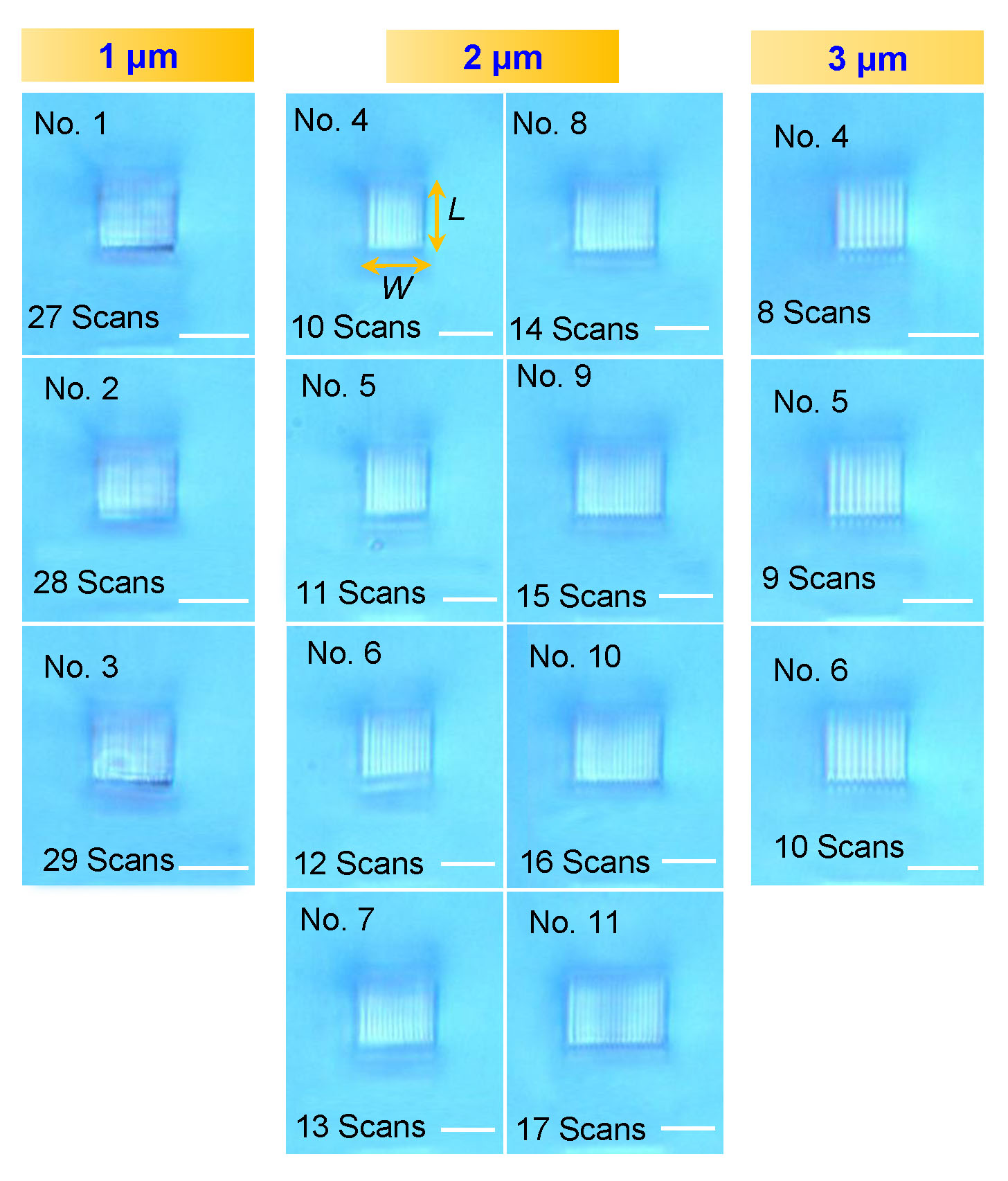
Figure 4 Microscope images of multi-line optical waveguides in LiTaO3 crystals under parallel polarization. Left panel: trace intervals of 1 μm with 27-29 traces; middle panel: trace intervals of 2 μm with 10-17 traces; right panel: trace intervals of 3 μm with 8-10 traces.
Figure 5 shows microscope images of three sets of multi-line optical waveguides fabricated with different trace intervals under perpendicular polarization. The intervals between traces No.15-No.18 are 1 μm, No.19-No.25 are 2 μm, No.26-No.28 are 3 μm, among them, No.19 has an end-face dimension of 14.46×14.63 μm2, which is the closest to a square symmetric structure.
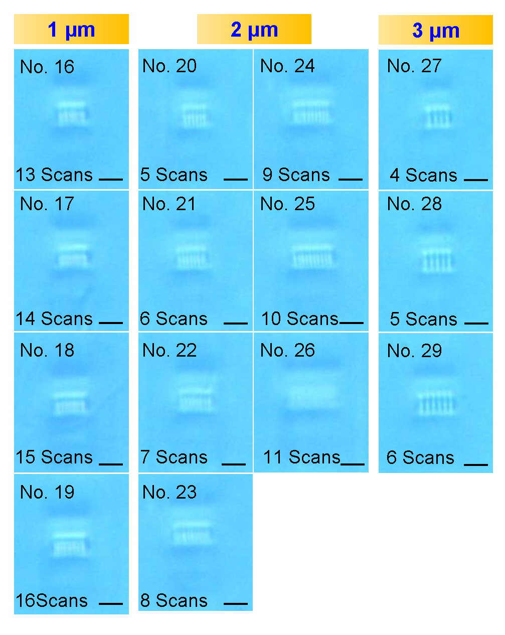
Figure 5 Microscope images of multi-line optical waveguides in LiTaO3 crystals under perpendicular polarization. Left panel: trace intervals of 1 μm with 13-16 traces; middle panel: trace intervals of 2 μm with 5-11 traces; right panel: trace intervals of 3 μm with 4-6 traces.
End-face coupling experiments were conducted employing He-Ne and 4-λ fiber lasers as light sources, near-field mode profiles at 633 nm and 1550 nm wavelengths respectively. Figure 6 and Figure 7 show the near-field mode distributions along the TM direction at 633 nm and 1550 nm under parallel and perpendicular polarization, respectively. We demonstrate that controlling the number of writing traces enables tailored manipulation of the modal distribution. Under parallel polarization, the mode at 633 nm exhibits a multimode distribution, while achieving TM00 fundamental mode transmission at 1550 nm. Under perpendicular polarization with a trace spacing of 2 μm, the mode at 633 nm evolves from the fundamental mode to multimode transmission as the number of traces increases. Only waveguides with a trace spacing of 1 µm support transmission at 1550 nm, while those with 2 μm and 3 μm spacings fail to meet the refractive index requirements for mid-infrared band confinement. Insertion loss measurements reveal that the losses under parallel polarization are significantly lower than those under perpendicular polarization, which is attributed to the larger waveguide cross-sectional dimensions. Furthermore, Waveguide No. 8 exhibits an insertion loss as low as 1.29 dB at 633 nm.
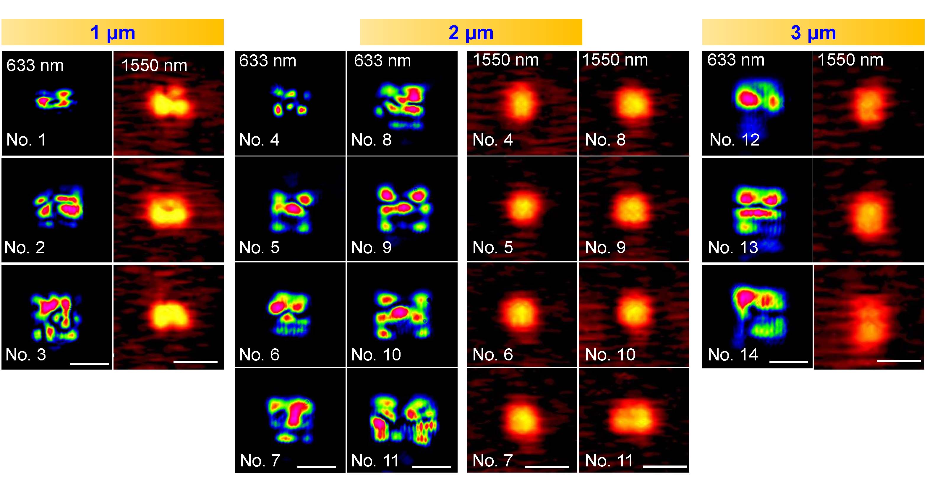
Figure 6 The near-field mode distributions of multi-line optical waveguides in LiTaO3 crystals under parallel laser polarization along the TM direction at 633 nm and 1550 nm.
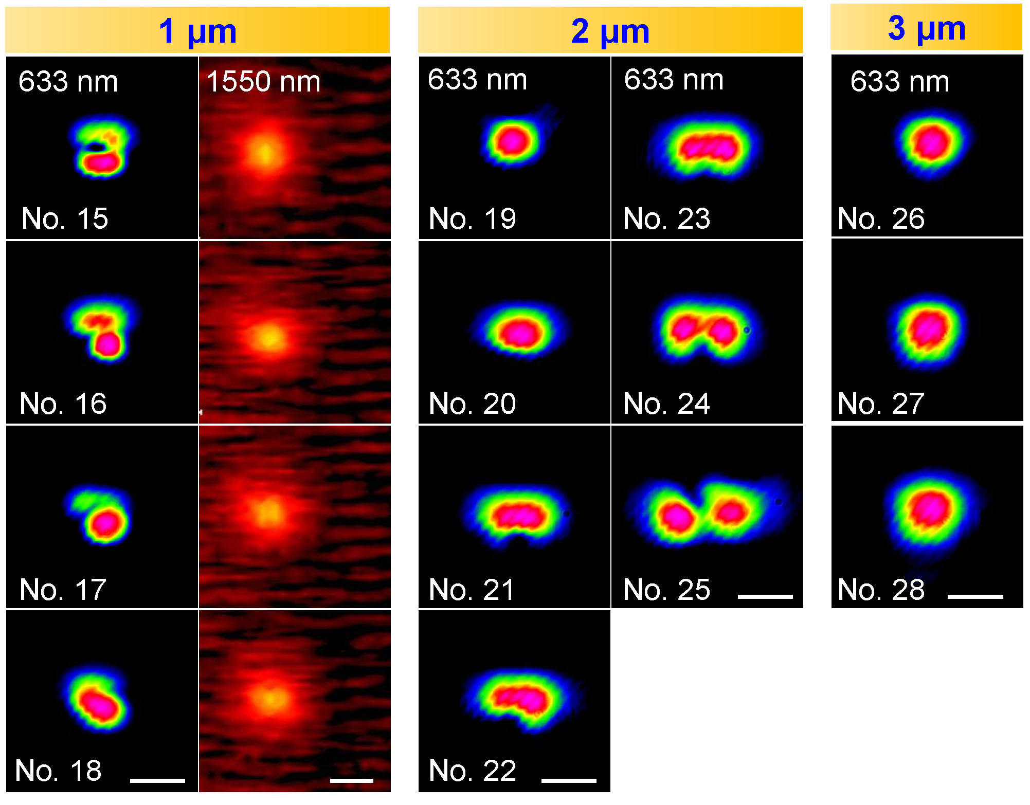
Figure 7 The near-field mode distributions of multi-line optical waveguides in LiTaO3 crystals under perpendicular laser polarization along the TM direction at 633 nm and 1550 nm.
4. Conclusion
In this paper, Type I single-line and multi-line optical waveguides based on refractive index increase modification are fabricated in LiTaO₃ crystals, and the factors influencing the success or failure of high-performance waveguides fabrication are investigated. By adjusting the writing parameters, a smooth and uniform transition from Type I refractive index increase modification to Type II lattice damage with refractive index decrease modification is achieved. By utilizing multiple scanning techniques, the cross-sectional profile of the waveguide is controlled to exhibit either a square or circularly symmetric distribution, enabling the tailoring of waveguide modes. The single-line optical waveguide exhibits a low insertion loss of 1 dB at 633 nm, while the multi-line optical waveguide supports efficient guided-mode propagation at the communication wavelength of 1.55 μm. The optical waveguides fabricated based on this Type I refractive index modification exhibit advantages such as simple structure, direct writing capability and high flexibility, which enables the fabrication of complex optical waveguide devices through direct three-dimensional scanning of the sample, facilitating their application in quantum chip information technology.
Conflicts of Interest
The authors declare no conflict of interest.
Acknowledgements
This work was supported by the National Natural Science Foundation of China (NSFC) (No. 12204261), Shandong Province Natural Science Foundation (No. ZR2022QA059), China Postdoctoral Science Foundation(2023M731850), and National Key Research and Development Program of China (2023YFF0715100, 2023YFF0715105).
Author contributions
Lijuan Shi: Conceptualization, Investigation, Experiment, Writing-original draft. Pengda Wang: Experiment, Calculation, Validation. Kun zhang: Review and editing. Lingqi Li: Wriitng, review and editing. Kongwei Jin: Supervision.
References
D. Du, X. Liu, G. Korn, J. Squier, G. Mourou. "Laser-induced breakdown by impact ionization in SiO2 with pulse widths from 7 ns to 150 fs." Appl. Phys. Lett. 1994, 64, 23, 3071-3073.
R. R. Gattass, E. Mazur. "Femtosecond laser micromachining in transparent material." Nat. Photonics 2008, 2, 4, 219-225.
K. Sugioka, Y. Cheng. "Femtosecond laser three-dimensional micro-and nanofabrication." Appl. Phys. Rev. 2014, 1, 4.
S. Gross, M. J. Withford. "Ultrafast-laser-inscribed 3D integrated photonics: challenges and emerging applications." Nanophotonics 2015, 4, 3, 332-352.
F. Sima, K. Sugioka, R. M. Vazquez, R. Osellame, L. Kelemen, P. Ormos. "Three-dimensional femtosecond laser processing for lab-on-a-chip applications." Nanophotonics. 2018, 7, 3, 613-634.
A. Arai, J. Bovatsek, F. Yoshino, Z. Liu, G. C. Cho, L. Shah, M. E. Fermann, Y. Uehara. "Fiber chirped pulse amplification system for micromachining." Conference Proceedings Article, 2006, 6343, 226-237.
B. N. Chichkov, C. Momma, S. Nolte, F. von Alvensleben, A. Tünnermann. "Femtosecond, picosecond and nanosecond laser ablation of solids." Appl. Phys. A 1996, 63, 2, 109-115.
Y. Nakata, T. Okada, M. Maeda. "Lithographical laser ablation using femtosecond laser." Appl. Phys. A. 2004, 79, 1484-1483.
K. M. Davis, K. Miura, N. Sugimoto, K. Hirao. "Writing waveguides in glass with a femtosecond laser." Opt. Lett. 1996, 21, 21, 1729-1731.
S. X. Guo, F. Bourgeois, T. Chokshi, N. J. Durr, M. A. Hilliard, N. Chronis, A. Ben-Yakar. "Femtosecond laser nanoaxotomy lab-on-a-chip for in vivo nerve regeneration studies." Nat. Methods 2008, 5, 6, 531-533.
H. Tang, X. F. Lin, Z. Feng, J. Y. Chen, J. Gao, K. Sun, C. Y. Wang, P. C. Lai, X. Y. Xu, Y. Wang. "Experimental two-dimensional quantum walk on a photonic chip." Sci. Adv. 2018, 4, eaat3174.
Y. Chen, J. Gao, Z. Q. Jiao, K. Sun, W. G. Shen, L. F. Qiao, H. Tang, X. F. Lin, X. M. Jin, "Mapping Twisted Light into and out of a Photonic Chip." Phys. Rev. Lett. 2018, 121, 233602.
N. Spagnolo, C. Vitelli, M. Bentivegna, D. J. Brod, A. Crespi, F. Flamini, S. Giacomini, G. Milani, R. Ramponi, P. Mataloni. "Experimental validation of photonic boson sampling." Nat. Photonics 2014, 8, 8, 615-620.
N. Spagnolo, C. Vitelli, L. Aparo, P. Mataloni, F. Sciarrino, A. Crespi, R. Ramponi, R. Osellame. "Three-photon bosonic coalescence in an integrated tritter." Nat. Communications 2013, 4. 1-6.
J. Burghoff, S. Nolte, A. Tünnermann. "Origins of waveguiding in femtosecond laser-structured LiNbO3." Appl. Phys. A 2007, 89, 1, 127-132.
K. Sugioka, Y. Cheng. "Femtosecond laser three-dimensional micro- and Nanofabrication." Appl. Phys. Rev. 2014, 1, 4. 041303.
F. Chen, J. R. Vázquez de Aldana, Laser. "Optical waveguides in crystalline dielectric materials produced by femtosecond-laser micromachiningLaser." Laser. Photonics. Rev. 2014, 8, 2, 251-275.
I. Dolev, A. Ganany-Padowicz, O. Gayer, A. Arie, J. Mangin, G. Gadret. "Linear and nonlinear optical properties of MgO:LiTaO3." Appl. Phys. B 2009, 96, 2-3, 423-432.
L. Tokodi, A. Buzady, J. Hebling, L. Palfalvi. "Possibility of high-energy THz generation in LiTaO3." Appl. Phys. B 2016, 122, 9, 235.
N. E. Yu, S. Kurimura, Y. Nomura, M. Nakamura, K. Kitamura, Y. Takada, J. Sakuma, T. Sumiyoshi. "Efficient optical parametric oscillation based on periodically poled 1.0 mol % MgO-doped stoichiometric LiTaO3." Appl. Phys. Lett. 2004, 85, 22, 5134-5136.
K. Lee, D. Ko, N. E. Yu. "Temperature-dependent Sellmeier equation at terahertz frequency range for 1 mol % MgO-doped stoichiometric lithium tantalate." Jpn. J. Appl. Phys. 2017, 56, 4. 040303.
M. K. Shukla, S. Kumar, R. Das. "Single-Pass Multi-Watt Second-Harmonic-Generation in Congruent and Stoichiometric LiTaO3." IEEE Photonic. Tech. L. 2015, 27, 13, 1379-1382.
L. Wang, X. Zhang, L. Li, Q. Lu, C. Romero, J. R. Vázquez de Aldana, F. Chen. "Second harmonic generation of femtosecond laser written depressed cladding waveguides in periodically poled MgO : LiTaO3 crystal." Opt. Express 2019, 27, 3, 2101-2111.
M. Triplett, J. Khaydarov, X. Xu, A. Marandi, G. Imeshev, J. Arntsen, A. Ninan, G. Miller, C. Langrock. "Multi-watt, broadband second-harmonicgeneration in MgO: PPSLT waveguides fabricated with femtosecond laser Micromachining." Opt. Express 2019, 27, 15, 21102-21115.
L. Li, W. Nie, Z. Li, B. Zhang, L. Wang, P. Haro-Gonzalez, D. Jaque, J. R. Vázquez de Aldana, F. Chen. "Femtosecond Laser Writing of Optical Waveguides by Self-Induced Multiple Refocusing in LiTaO3 Crystal." J. Lightwave Technol. 2019, 37, 14, 3452-3458.
D. Ashkenasi, H. Varel, A. Rosenfeld, S. Henz, J. Herrmann, E. E. B. Cambell. "Application of self-focusing of ps laser pulses for three-dimensional microstructuring of transparent materials." Appl. Phys. Lett. 1998, 72, 12, 1442-1444.
T. Meany, M. Gräfe, R. Heilmann, A. Perez-Leija, S. Gross, M. J. Steel, M. J. Withford, A. Szameit. "Laser written circuits for quantum photonics." Laser Photonics Rev. 2015, 9, 4, 363-384.
W. Ryba-Romanowski, B. Macalik, A. Strzep, R. Lisiecki, P. Solarz, R. M. Kowalski. "Spectral transformation of infrared ultrashort pulses in laser crystals." Opt. Mater. 2014, 36, 10, 1745-1748.