



Beyond Resolution: Recent Progress and Industrial Challenges of Nanoimprint Lithography for Advanced Semiconductor Manufacturing
Vol. 2. Issue 3. | published: 18 July 2026
DOI: https://doi.org/10.63174/xdi.NZLB4235 | Get PDF
Abstract
The relentless downscaling of semiconductor devices has pushed conventional lithography toward both economic and physical limits. Deep Ultraviolet (DUV) lithography with multi-patterning schemes causes exponential cost escalation, while Extreme Ultraviolet (EUV) lithography imposes prohibitive capital investment exceeding US$150 million per scanner and megawatt-scale power consumption. Within this landscape, nanoimprint lithography (NIL) has re-emerged as a compelling complementary patterning technology. Unlike projection-based methods, NIL achieves pattern definition through mechanical contact and material displacement. Therefore, it bypasses optical diffraction limits and stochastic effects caused by photo-shot noise. This review provides a systematic evaluation of the transition of NIL from laboratory demonstration to semiconductor high-volume manufacturing (HVM), with emphasis on progress made during 2023-2025. We highlight the paradigm shift from resolution-centric studies to manufacturing-driven metrics including overlay accuracy, defect density, throughput, template lifetime, residual layer uniformity, and cost of ownership (CoO). We then examine recent advances across six key technology modules: tool architecture, overlay improvement, defect suppression, template ecosystems, resist engineering, and application-specific integration. We argue that NIL is positioned as a high-value strategic complement targeting specific layers in DRAM, 3D NAND, and advanced packaging, where sub-10 nm resolution, three-dimensional patterning capability, and order-of-magnitude lower cost-of-ownership provide decisive advantages. The review concludes by projecting potential trajectory of NIL through 2028, identifying template ecosystem maturation, artificial intelligence-driven process optimization, and hybrid mix-and-match lithography strategies as critical factors for adoption.
1. Introduction
The global semiconductor industry stands at a critical inflection point. For over five decades, Moore's Law has been sustained by continuous advances in optical projection lithography, enabling the exponential growth in transistor density that underpins modern computing, communications, and artificial intelligence. However, as feature dimensions approach the atomic scale, the economic and physical foundations of this scaling model are being fundamentally challenged [1,2]. The industry now confronts a structural tension. Historically, the cost per transistor decreased with each new technology generation. At advanced nodes, this trend has weakened or even reversed because lithographic patterning has become increasingly complex. An emerging consensus recognizes that no single lithographic technology can universally address all patterning requirements. Thus, a mix-and-match approach that combines complementary technologies is increasingly essential [39].
Current leading-edge manufacturing relies on 193 nm immersion (193i) lithography. Its resolution has been extended through complex multi-patterning schemes, including self-aligned double patterning and self-aligned quadruple patterning, to achieve sub-38 nm half-pitch features [3,4]. Although these approaches are effective, each additional patterning step compounds capital investment, process complexity, overlay error accumulation, and defect risk. A modern 193i scanner costs approximately US$50–70 million, and the associated consumables, metrology, and process control infrastructure can double the effective cost per wafer pass. For foundries operating at the 7 nm node and below, lithography-related processes now account for over half of total wafer processing costs.
Extreme ultraviolet (EUV) lithography, operating at 13.5 nm wavelength, was introduced to address this scaling challenge. A single EUV scanner with high numerical aperture (NA) costs US$150–200 million and consumes approximately 1.5 MW of power per tool due to its inherent low wall-plug efficiency and conversion efficiency below 5%. EUV also introduces stochastic defect mechanisms including photon shot noise and secondary electron blur that become dominant yield limiters at sub-10 nm critical dimensions. The resulting high cost of ownership (CoO) has created an economic segmentary situation: not every patterned layer can economically justify EUV's capabilities. A substantial patterning-cost gap has thus emerged, particularly, for instance, in high-density array layers of Dynamic Random Access Memory (DRAM), complex deep-trench structures in 3D NAND flash memory, dual damascene interconnects in back-end-of-line processing, and high-density redistribution layers in advanced packaging. These layers require resolution beyond single-exposure DUV capability, yet their cost structures cannot absorb EUV's overhead. Recent analyses of lithography cost dynamics have systematically quantified this gap in detail [38].
Nanoimprint lithography (NIL) has re-emerged as a promising solution to address this cost-resolution gap. It was first demonstrated by Chou et al. in 1995-1996 with 25 nm resolution using thermal imprinting into poly(methyl methacrylate) (PMMA) [5,6]. This work established a fundamentally different patterning technique based on pure mechanical replication. The subsequent development of UV-curable NIL by Haisma et al. [7] and step-and-flash imprint lithography (S-FIL) by Colburn et al. [8] enabled room-temperature processing with low-viscosity, photocurable liquid resists. This was a critical innovation that avoided the imprint process from thermal expansion effects and enabled the overlay precision necessary for multilayer semiconductor devices [9]. Over three decades of development, NIL has evolved into a technology with proven sub-10 nm resolution, high-throughput capability, and an order-of-magnitude lower energy consumption and cost per wafer compared to EUV [10,11]. Schift described NIL as extending beyond conventional lithography into a versatile manufacturing platform capable of direct functional patterning across diverse domains including photonics, biotechnology, and other fields [12]. Multiple analyses have further suggested that NIL can reduce per-layer patterning cost by 40–50% compared to EUV single-exposure in selected memory applications [40].
The year 2023 marked an important milestone: Canon Inc. announced the FPA-1200NZ2C, the first semiconductor-grade NIL system worldwide built for 300 mm wafer manufacturing [28]. This system employs Jet and Flash Imprint Lithography (J-FIL) technology described by Sreenivasan [13]. It achieves 14 nm half-pitch resolution corresponding to the 5 nm logic node, with a demonstrated extendibility path to 10 nm resolution corresponding to the 2 nm node. The overlay accuracy below 3 nm and throughput of eighty wafers per hour represent dramatic improvements that pushed NIL from a research concept into a viable manufacturing candidate. Canon shipped the first unit to the Texas Institute for Electronics in late 2024 [29]. Other major semiconductor manufacturers including Kioxia, Toshiba, SK Hynix for 3D NAND, and Micron Technology for DRAM are actively evaluating NIL for production insertion [10,14]. This commercial momentum is supported by progress in the supply chain. For instance, DNP has demonstrated 10 nm line-pattern resolution on production-grade templates [37], and Fujifilm has introduced dedicated NIL resist products [41].
This review provides a systematic assessment of NIL progress toward semiconductor HVM, with focus on the transformative advances achieved through 2023-2025. Unlike prior reviews that mainly have emphasized resist chemistry or individual demonstrations, this review evaluates NIL using metrics relevant to real fabrication lines to the most up-to-date extent. Section 2 discusses the shift from laboratory-oriented metrics to manufacturing-oriented criteria. Section 3 reviews recent progress across six key technology modules. Section 4 examines the main barriers to industrialization. Section 5 discusses future opportunities and likely adoption pathways.

Figure 1. Evolution of nanoimprint lithography from laboratory demonstration to high-volume manufacturing. The timeline traces key milestones from Chou's seminal 1995 demonstration through Canon's 2023 semiconductor-grade FPA-1200NZ2C tool, illustrating the progressive maturation from academic research to industrial deployment.
2. From Laboratory to Fab: The Paradigm Shift in NIL Evaluation Metrics
During the first two decades of development, NIL was mainly evaluated through a resolution-centric lens. In laboratory research, a successful imprint was often defined as the faithful replications of the template topography on a small, rigid, planar substrate, typically a silicon chip in a size of a few square centimeters. Process uniformity across larger scales or compatibility with full semiconductor process flows were often secondary concerns.
These early studies were essential because they demonstrated the intrinsic resolution capability of mechanical patterning. However, they also underestimated the multidimensional requirements of semiconductor manufacturing, such as its ability to maintain yield, uniformity, and compatibility throughout the full process flow [9,13]. Recent wafer-scale NIL studies have begun to demonstrate viable overlay performance at full-wafer dimensions [42].
The transition to semiconductor HVM demands a fundamentally different evaluative framework. In a modern wafer fabrication facility processing 50,000 to 100,000 wafer starts per month, printing a nanoscale feature represents merely the baseline requirement. Real industrial viability is dictated by yield- and cost-driven metrics that must be simultaneously satisfied, which includes overlay accuracy, defect density, throughput, template lifetime, residual layer uniformity, and CoO. Any single dimension falling outside specification can render the entire process economically non-feasible, regardless of performance in the remaining dimensions. Each of these critical HVM metrics is examined below in Figure 2.
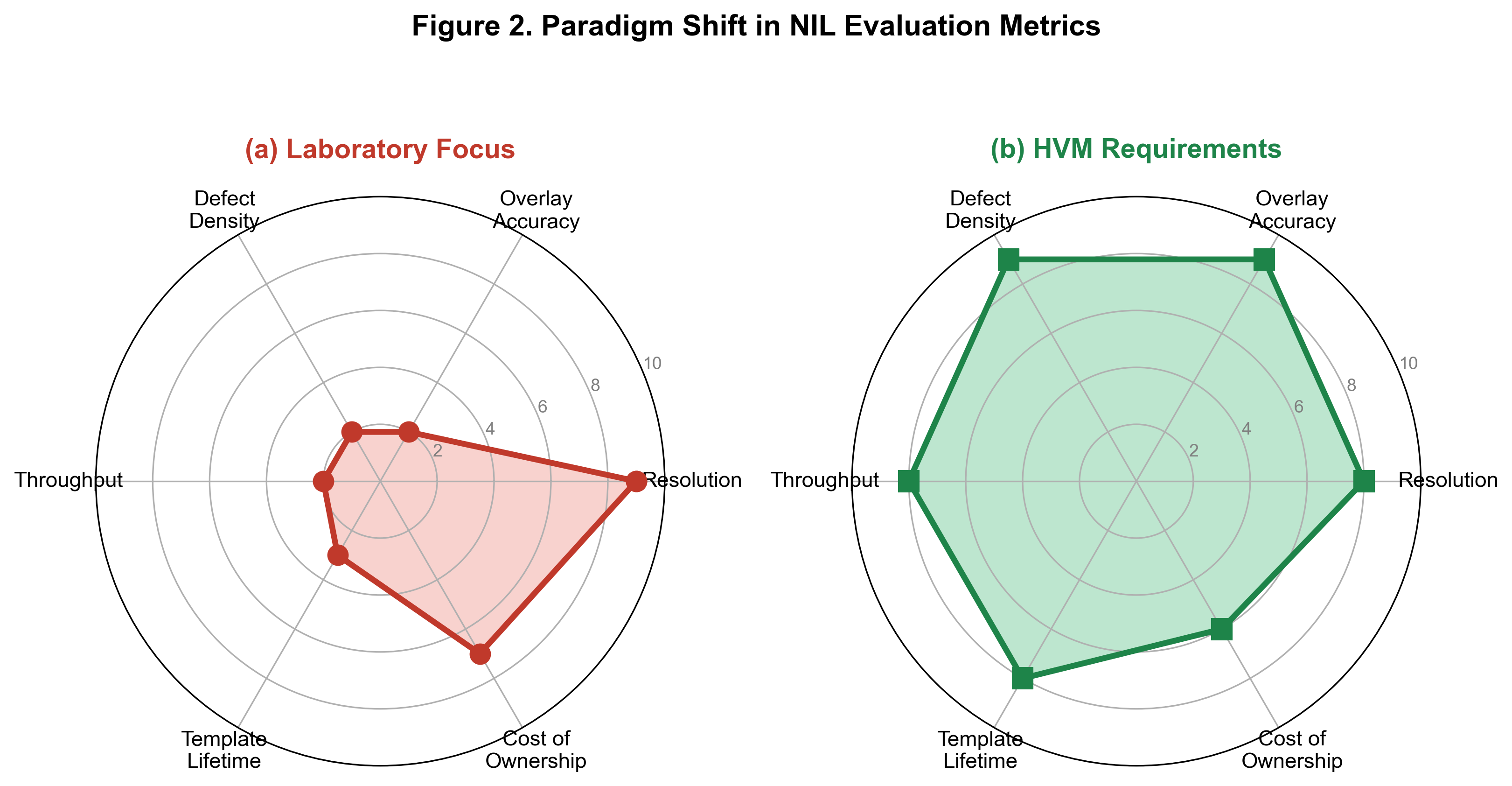
Figure 2. Paradigm shift in NIL evaluation metrics from laboratory to high-volume manufacturing. (a) Laboratory focus prioritizes ultimate resolution, often at the expense of other manufacturability metrics. (b) HVM demands balanced, simultaneous performance across overlay accuracy, defect density, throughput, template lifetime, and CoO. An excursion in any single dimension can render the entire process economically nonviable.
2.1 Overlay Accuracy
In semiconductor manufacturing, dozens of patterned layers must be stacked with nanometer-level precision. The overlay budget is typically less than one quarter of the minimum half-pitch, leading to single-digit nanometer tolerances [13]. For instance, for DRAM at the 1x nm node, the overlay tolerant is expected to be 3-5 nm; for leading-edge logic at 3 nm and below, budgets shrink to 1-1.5 nm.
These requirements are non-negotiable, as lacking overlay accuracy can directly cause device failure through short circuits, open circuits, or parametric degradation. Unlike projection lithography, NIL relies on direct mechanical contact. Error sources including template elastic deformation, wafer distortion, thermal drift, resist shrinkage of five to ten percent for acrylate systems, and mechanical relaxation upon demolding can be introduced [15,16]. Managing these coupled thermo-mechanical-chemical effects while achieving sub-3 nm overlay across an entire 300 mm wafer represents one of the greatest challenges of NIL industrialization [17].
2.2 Defectivity and Yield Compatibility
The contact-based nature of NIL bypasses optical diffraction limits and photon-driven stochastic effects. However, it introduces mechanical defects that are absent in non-contact patterning. Memory devices may tolerate approximately one to ten defects per square centimeter, while logic circuits require much more strict defect control, i.e., 0.01 to 0.1 defect per square centimeter [13].
As shown in Figure 3, NIL-specific defect modes can be grouped into four categories: (a) template-related defects, including particle transfer, pattern wear, and anti-sticking coating degradation; (b) fill-related defects, such as voids, bubble entrapment, and residual layer thickness (RLT) anomalies; (c) demolding-related defects, including pattern fracture, residue, collapse, and blowout; and (d) integration-related defects, which may be amplified during subsequent etching, metallization, and chemical-mechanical polishing (CMP) [14,31].
Defect control has been a central focus of industrial NIL development in recent years. Progress has required coordinated improvements in tool design, materials, environment control, and process recipes. For instance, inkjet-based resist dispensing combined with optimized droplet recipes has proven particularly effective in reducing fill-related defects [43].

Figure 3. Exemplary classification of NIL defect sources in semiconductor manufacturing. Four principal defect categories are identified: (a) template-related defects from particle contamination, pattern wear, and coating degradation; (b) fill-related defects from gas entrapment and non-uniform droplet distribution; (c) demolding-related defects including pattern fracture and adhesive failure; (d) integration-related defects amplified during subsequent etching, metallization, and planarization processes. Corresponding mitigation strategies are summarized.
2.3 Template Lifetime and Cost Dynamics
In optical projection lithography, the photomask does not contact the wafer and thus can theoretically serve a very large number of exposures. In contrast, an NIL template functions simultaneously as a patterning master and a mechanical molding tool, which is subjected to repeated contact, pressure, UV exposure, and demolding cycles.
A single industrial master template fabricated by electron-beam lithography (EBL) can cost US$50,000–100,000[18]. To reduce wear on the master, NIL typically uses a working stamp replication strategy, in which the expensive master is used to generate replica templates for production. However, the economic viability of this approach depends strongly on the lifetime of the replica. For HVM, each working template is expected typically to survive thousands of imprint cycles. Lifetimes of 5,000–10,000 wafer imprints are often viewed as a critical target.
2.4 Process Integration and Residual Layer Control
In NIL process, a thin film of cured resist, referred to residual layer, remains at trench bottoms after imprint. The residual layer thickness (RLT) must be tightly controlled. Spatial variations in RLT directly produce critical dimension (CD) non-uniformity after etch transfer. For instance, a 2 nm variation in RLT can produce 1-3 nm CD variation, while sub-nanometer line edge roughness control remains critical for advanced nodes [23].
In HVM, NIL must also integrate smoothly with descumming, hardmask etching, pattern transfer, deposition, electroplating, CMP and so on. Any additional variability introduced at these stages can affect final device yield. Recent work has also demonstrated that combining inkjet printing with NIL enables better control of RLT uniformity across variable pattern densities [43].
2.5 Throughput and Fab Cadence
A modern semiconductor fab may process up to 100,000 wafers per month through hundreds of process steps. NIL must therefore meet stringent throughput and uptime requirements. For practical HVM, NIL is expected to sustain 80-120 wafers per hour with over 90% uptime [13]. J-FIL reaches high throughput by combining several fast process steps. It achieves approximately 10-15s per field through parallel inkjet dispensing, sub-second capillary filling, millisecond UV exposure, and automated demolding [28,14]. The development of solvent-based resists has been instrumental in pushing the throughput boundary while maintaining fidelity [30]. The commercial availability of dedicated NIL resists such as from Fujifilm further strengthens the supply chain [41].
3. Recent Progress in NIL for Advanced Semiconductor Manufacturing (2023-2025)
Building on the HVM evaluation framework established in Section 2 — which defined overlay accuracy (§2.1), defectivity (§2.2), template lifetime (§2.3), residual layer control (§2.4), and throughput (§2.5) as the critical manufacturing metrics — this section examines recent technical progress through the lens of six key technology modules. The mapping is as follows: tool architecture (§3.1) addresses throughput and residual layer uniformity; overlay improvement (§3.2) directly targets the overlay challenge; defect reduction (§3.3) corresponds to defectivity control; template technology (§3.4) addresses template lifetime and cost; resist engineering (§3.5) impacts residual layer control, throughput, and overlay; and application-specific integration (§3.6) contextualizes these modules within real manufacturing scenarios. Figure 4 displays NIL in a strategic resolution-cost landscape relative to established lithographic technologies.
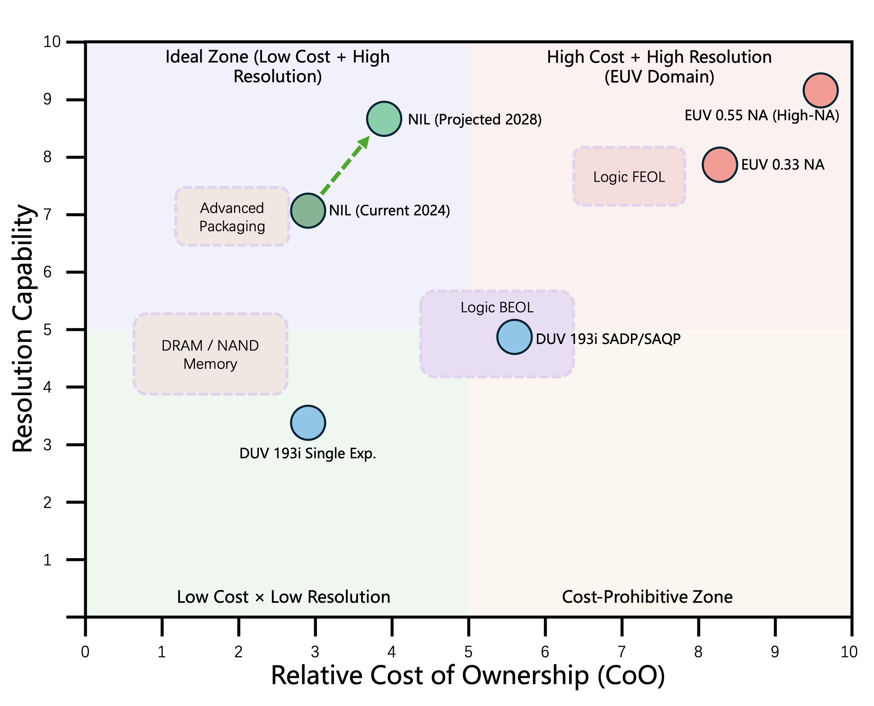
Figure 4. Comparative positioning of lithographic technologies in the resolution-cost landscape. DUV-based approaches (blue) offer low cost but limited resolutions. EUV-based approaches (red) deliver highest resolution at extreme capital and operational cost. NIL (green) occupies a unique position combining sub-10 nm resolution with an order-of-magnitude lower CoO. The dashed arrow indicates NIL's projected trajectory toward 2028 as template and process capabilities mature.
3.1 Tool Architecture and Field-Level Processing Strategies
The Canon FPA-1200NZ2C system operates on a step-and-repeat principle in a 26 mm * 33 mm field, matching the standard optical lithography field size [28,13]. The J-FIL process consists of four main stages: a) piezo-driven inkjets dispense sub-picoliter droplets with adaptive density matching; b) capillary forces and controlled template bowing drive progressive center-to-edge filling. Helium or carbon dioxide ambient atmospheres enhances gas dissolution and reduces bubble formation; c) a sub-second UV pulse cross-links the resist; d) a precision-controlled separation sequence releases the template from the cure resist [14,15].
A major advance has been the maturation of physics-based simulation, which is capable of coupling computational fluid dynamics, finite-element analysis, and reaction kinetics. It allows prioritization of droplet recipes for complex pattern layouts. In some cases, residual layer thickness uniformity within ±2 nm has been achieved across fields with arbitrary pattern densities [15]. The simulation-driven workflow can reduce the process development cycles from weeks to days. Figure 5 provides a visual overview of the nanoimprint lithography process from its origins to current semiconductor-grade implementation. Panel (a) presents the sequential micrographs of the silicon stamp with a 40-nm-period pillar array. Panel (b) illustrates the Step-and-Flash Imprint Lithography (SFIL) / Jet and Flash Imprint Lithography (J-FIL) process sequence. It depicts the four critical stages of inkjet-based adaptive resist dispensing onto a transfer layer, capillary-driven filling with controlled template bowing, UV cross-linking through the transparent template, and precision demolding separation followed by breakthrough and transfer etching. Panel (c) displays key modules of the production-grade J-FIL stepper system, including the multi-nozzle piezo inkjet array for sub-picoliter droplet dispensing and the nanometer-accuracy X-Y-θ motion stage. The template Magnification and Shape Correction System (MSCS) and the Interferometric Moiré Alignment Technology (i-MAT) ensure sub-nanometer detection at 4,500 Hz for sub-3-nm overlay performance.
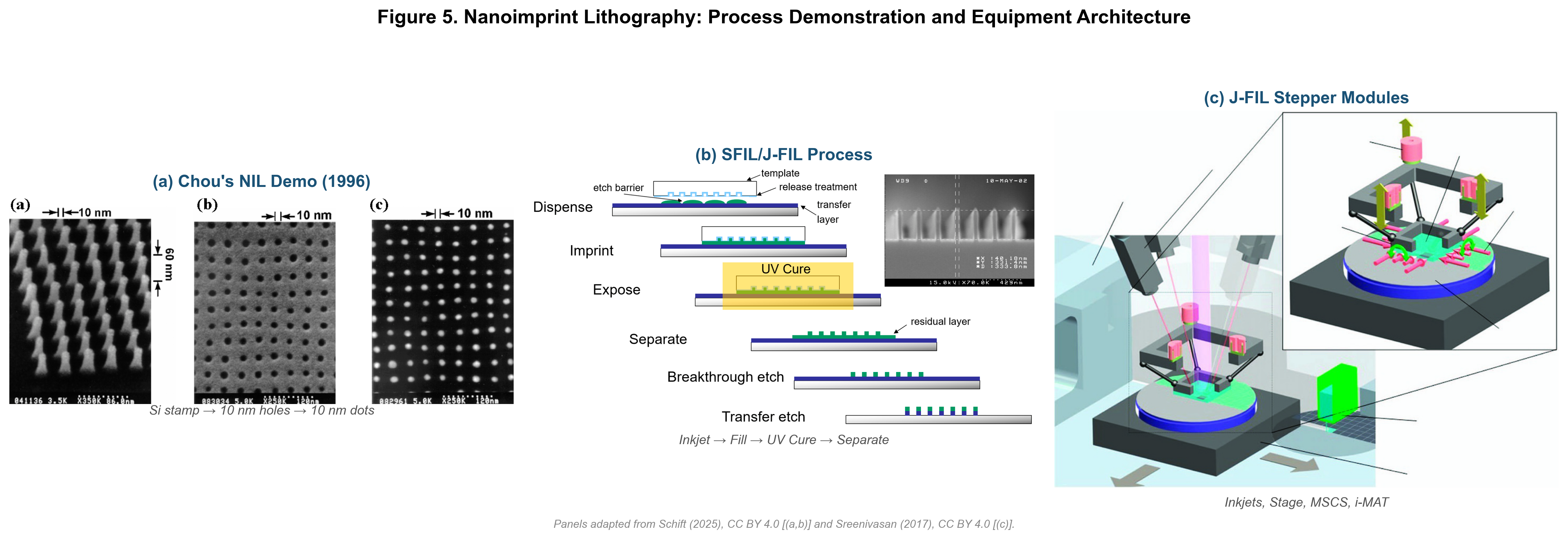
Figure 5. Nanoimprint lithography: process demonstration and equipment architecture. (a) Reproduction of Chou's original 1996 demonstration. (b) SFIL/J-FIL process sequence. Panels (a) and (b) adapted from Schift (2025), CC BY 4.0. (c) J-FIL stepper system critical modules. Adapted from Sreenivasan (2017), CC BY 4.0.
3.2 Overlay Improvement and Multi-Tier Distortion Correction
Overlay improvement has been one of the most important achievements in recent NIL development. The Interferometric Moiré Alignment Technique (i-MAT) from Canon achieves sub-nanometer detection at 4,500 Hz through Moire interferometry [13,17]. Overlay correction is performed in a hierarchical manner. Coarse alignment is first conducted before contact, typically to approximately 500 nm. Fine alignment is then performed after contact, reducing residual errors to the sub-10 nm range. Further correction is achieved through two complementary approaches. The first is magnification and shape correction using a multi-segment chucking system with 16 actuators. The second is high-order distortion correction using digital-micromirror-device-directed laser heating. This method locally adjusts field-level thermal expansion [17]. Looking beyond current production tools, emerging metrology approaches such as meta-device-based subwavelength displacement sensing may offer complementary pathways for overlay verification, while computational techniques developed for inverse lithography technology provide methodological insights applicable to NIL distortion compensation[26,27].
Recent results show a single-machine overlay reached 1.8 nm (x) and 1.5 nm (y) at 3σ. Matched-machine overlay with ASML ArFi tool achieved 2.4 nm (x) and 2.2 nm (y), demonstrating the feasibility of hybrid NIL-optical lithography flows [10,14]. For DRAM with overlay budgets of 3-4 nm, these values are within range. Overall, the overlay performance has been improved by approximately a factor of five over the past decade [17].
3.3 Defectivity Reduction
Defectivity has also improved substantially. The repeat defect density decreased from approximately 10 defects per wafer in 2013-era prototypes to 0.003 per wafer in 2024 production-grade tools, a reduction of over three orders of magnitude [10,14]. The improvement was enabled by several tool-level and process-level advances, including employing ceramic chamber materials, high efficiency particulate air filter (HEPA) plus laminar airflow, and electrostatic discharge neutralization [28,29].
Fill defects have been reduced through optimized template bowing, helium ambient processing, and solvent-based resists [30]. Recent work specifically demonstrates the effectiveness of combining inkjet printing with NIL for reduced non-fill defects [43]. Demolding defects are mitigated via separation trajectory control, using fluorinated anti-sticking coatings for a reduction of adhesion energy below 10 mJ/m². Limiting the pattern aspect ratio helps improving the demolding defect control as well. An aspect ratio below approximately 2.5:1 is often preferred [32].
Machine learning is becoming an important tool for defect analysis. Automated classification models have achieved accuracy above 95% [35]. Current reported defect density of 0.03 defects/cm² is approaching the regime required for selected memory applications [10].
3.4 Template Technology
Template fabrication technologies are critical to the industrialization of NIL. Hierarchical replication strategies can decouple the cost of the master template from production consumables, which significantly lowered the template-related CoO [10,18]. It is reported that master templates fabricated by DNP achieve sub-nanometer placement accuracy [37]. DNP has also demonstrated 10 nm line-pattern resolution, extending the roadmap to the 2 nm node [37].
Template repair is another important area of progress. Repair methods via multiple-patterning techniques may transform fatal defects into correctable anomalies [19]. Durable anti-sticking coatings, including diamond-like carbon variants, have demonstrated lifetimes exceeding 50,000 imprint cycles under selected conditions [32].
3.5 Resist Materials and Interface Engineering
NIL resists need to satisfy demanding and often conflicting requirements. In liquid state, the NIL resists are expected to have low viscosity, low volatility, and good filling behavior. A typical target viscosity is in the range of 1–5 cP. In solid phase, i.e. cured cross-linked state, the resist shall provide high mechanical strength, controlled adhesion, good etch resistance, and low shrinkage [13,33].
The acrylate-based chemistries remain nowadays dominant because of their rapid curing kinetics. Silicon-containing monomers can improve etch selectivity and solvent-borne formulations can achieve viscosity below 2 cP that enables a ultrafast filling [30]. However, resist shrinkage remains always a major concern. Shrinkage of 5-10% may consume a significant portion of the overlay budget. Ring-opening chemistries offer a possible route to near-zero shrinkage but comes at the cost of slower kinetics[34]. The commercial availability of NIL-specific resists from suppliers such as Fujifilm represents important ecosystem maturation [41]. In parallel, physics-based process simulation has enabled improved residual layer control, with reported uniformity within approximately ±2 nm [23].
3.6 Application-Specific Process Integration
Memory applications, particularly 3D NAND and DRAM, represent currently the most advanced integration frontier [10,20]. The memory layers are attractive because they often combine dense, periodic patterns with strong cost pressure. Kioxia, Toshiba, SK Hynix for 3D NAND and Micron for DRAM conduct active evaluations.
Back-end-of-line (BEOL) dual damascene interconnects are another promising application benefiting from NIL, as it can directly form quasi 3D, more precisely 2.5D, resist profile. This enables simultaneous via-and-trench patterning and can collapse multiple patterning steps into one single imprint step, achieving approximately 40% cost reduction suggested by preliminary studies [14,22].
Advanced packaging applications also provide valuable insertion pathways, including redistribution layer patterning, hybrid bonding interfaces, and high-density interconnect structures [36]. The applications mentioned above may have more relaxed overlay requirements than leading-edge logic front-end layers, while still benefiting from NIL’s resolution and cost advantages.
Beyond traditional semiconductor applications, NIL has established commercial footholds in not only industrial products but also in consumer electronics, like metalens, AR/VR waveguide, and flexible optoelectronics [24,42,43,44]. Scalable NIL processes have been used to pattern large-area metasurfaces, showing strong potential for next-generation optical components [43,44]. These non-CMOS applications can accelerate tool learning, materials development, and ecosystem growth. Figure 6 synthesizes the application landscape and strategic positioning of NIL in semiconductor manufacturing. Panel (a) illustrates the strategic positioning framework: an inner ring anchored by sub-10-nm resolution and intrinsic three-dimensional patterning capability, a middle ring representing the lower CoO (~40–50% reduction) compared to EUV, and an outer temporal ring highlighting the memory-first adoption timeline in 2026–2027. Panel (b) presents a manufacturing readiness assessment across six key application domains, revealing that 3D NAND flash memory and AR/VR waveguides (both scoring 8/10) represent the most mature insertion opportunities, followed by DRAM arrays (7/10), advanced packaging (6/10), and logic BEOL interconnects (5/10). Flat optics and metalenses (9/10) represent the most mature non-CMOS application domain. Panel (c) quantitatively compares the process-step complexity of conventional optical dual damascene with NIL-based single-step BEOL interconnect formation, demonstrating an approximately 40% reduction in total process steps achieved by collapsing multiple lithography-etch sequences into a single imprint-and-transfer operation.
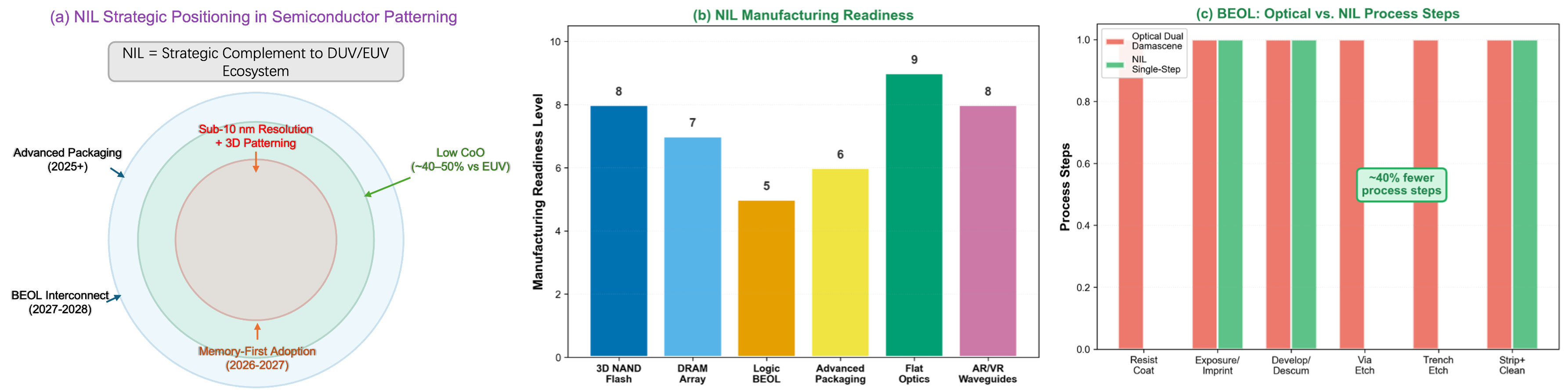
Figure 6. NIL applications and strategic positioning in semiconductor manufacturing. (a) Strategic positioning framework highlighting sub-10-nm resolution, cost advantages, and memory-first adoption in 2026-2027. (b) Manufacturing readiness assessment across six application domains. (c) Process step comparison between optical dual damascene and NIL single-step BEOL interconnect formation.
4. Industrialization Barriers: A Realistic Assessment
Despite rapid progress, NIL still faces systemic barriers to broad semiconductor adoption. It involves fundamental physical limits, capital requirements, supply chain immaturity, and the inertial forces of an industry that has invested hundreds of billions of dollars in established lithographic ecosystems. NIL shall therefore demonstrate not only technical feasibility, but also clear economic and manufacturing value in tools, materials, process flows, and design rules [41].
4.1 Overlay Limits
Current overlay of approximately 1.5 nm to 2.4 nm suits well for memory applications (typically 3-10 nm required) and is approaching the requirement for selected BEOL layers (typically 2-4 nm). Nevertheless, front-end logic layers below 3 nm node may require an overlay accuracy below 1.5 nm, which remains challenging for contact-based processes [13,17].
A fundamental issue arises from the coupling between imprint force and elastic deformation generated during mechanical contact of the template with the wafer. This inherent consequence of contact-based patterning represents a fundamental trade-off: it limits overlay accuracy, but also productively delineates NIL's most advantageous application domains — namely, layers with dense patterns, moderate overlay budgets, and strong cost sensitivity.
4.2 Defect Density and Contamination
Reported defect density of approximately 0.03 defects/cm[2] is promising for selected memory applications. However, more demanding logic applications require stricter defect control. Long-term stability over production volumes remains the key validation step [13].
Further consideration should be taken as many reported demonstrations use relatively regular test structures. Product wafers contain more diverse layouts, pattern densities, and topographies. Defect control must therefore be demonstrated under realistic integration conditions.
4.3 Template Supply Chain
Template supply is one of the most important industrial bottlenecks. It is reported that a high-volume memory fab could require 250-500 NIL templates per month, while the current global capacity appears much lower, approximately one-third of this projected demand [18,38].
This creates a classic chicken-and-egg problem. Device manufacturers hesitate to commit without a reliable template supply chain. At the same time, template suppliers may hesitate to expand capacity before clear production demand emerges. Overcoming this barrier will require coordinated investment across tool vendors, template manufacturers, materials suppliers, and device makers.
4.4 Ecosystem Maturity
Optical lithography benefits from over five decades of ecosystem development, ranging from scanner vendors, mask shops, resist suppliers, metrology tools, to computational lithography software, and mature design-for-manufacturing rules. NIL is building a comparable infrastructure from a much smaller base, and the integration of NIL into semiconductor industries requires multi-million-dollar investment before demonstrated production yield data [38].
In a comprehensive ecosystem, several components remain yet immature. Resist suppliers are still limited. Template inspection and repair tools require further development. Design rules for NIL-compatible layouts are still at an early stage. These ecosystem factors may slow adoption even when tool-level performance appears promising.
4.5 Strategic Positioning
There is broad consensus that NIL is unlikely to replace optical lithography as a universal patterning technology. NIL's most compelling value lies in specific layers satisfying such conditions: resolution beyond single exposure 193i capability, EUV economically prohibitive, high pattern density and periodicity, and overlay within NIL's demonstrated window. This view reflects a maturing understanding of NIL’s role [10,12,14]. Instead of a direct replacement for optical photolithography, NIL should be regarded as a strategic complement to DUV and EUV and is highly expected to perform well in that role.
4.6 Barrier Categorization: Near-Term Solvable vs. Structural Challenges.
The barriers discussed in Sections 4.1–4.5 can be categorized into two groups distinguished by their resolution trajectories. Category I — Actively Being Resolved (near-term, 2025–2027): (i) Defect density: improved from ~10/wafer (2013-era prototypes) to 0.003/wafer (2024 production-grade tools), approaching memory requirements; (ii) Resist ecosystem maturation: Fujifilm's NIL-specific resist launch (2024) and solvent-based formulations enabling sub-2 cP viscosity represent concrete supply chain progress; (iii) Overlay improvement: single-machine overlay reaching 1.5–1.8 nm (3σ) is within DRAM requirements. These barriers are on clear improvement trajectories supported by ongoing industrial investment. Category II — Requiring Structural Coordination (medium-term, 2027–2030): (i) Template supply chain scaling: current global capacity remains ~1/3 of projected HVM demand, requiring coordinated investment across tool vendors, template manufacturers, and device makers; (ii) Design rule development: NIL-compatible design-for-manufacturing rules remain nascent; (iii) Template inspection and repair infrastructure: still an emerging ecosystem component requiring dedicated tool development. This categorization directly informs the outlook discussion in Section 5.
5. Opportunities and Future Outlook
Memory-first adoption appears to be the most likely initial pathway for NIL high-volume manufacturing. The first production insertion may occur in the 2026–2027 timeframe, most likely in selected 3D NAND or DRAM layers [10,20]. These applications offer a favorable combination of pattern regularity, cost sensitivity, and relatively accessible overlay requirements.
The template ecosystem encompassing fabrication, inspection, repair, cleaning, and lifecycle management will be the single most critical determinant of commercial scalability [19]. Without a scalable and cost-effective template supply chain, NIL adoption will remain limited, even if tool performance continues to improve.
Artificial intelligence and machine learning are emerging as powerful cross-cutting enablers. Convolutional neural networks (CNN) can achieve over 95% accuracy in defect classification. Reinforcement learning may help identify process windows that are difficult to find through traditional design-of-experiment methods [35]. AI-assisted optimization could be especially useful for droplet recipe design, residual layer control, overlay correction, and predictive maintenance.
Hybrid mix-and-match strategies are likely to represent the most realistic deployment model, in which NIL handles specific high-density, cost-sensitive layers while optical lithography is retained for layers with the most stringent overlay requirements [10,12]. Such hybrid flows can exploit the strengths of each technology while limiting their weaknesses.
Beyond traditional CMOS scaling, NIL can be well positioned for emerging domains including metalens fabrication, AR/VR photonics, flexible electronics, and biomedical sensors [10,24,42,43,44]. These applications provide strategically valuable insertion pathways that can accelerate manufacturing learning and ecosystem development.
Nanoimprint lithography (NIL) has reached a genuine historic inflection point. Three decades after Chou's seminal demonstration, NIL has successfully transitioned from a laboratory concept into a credible, production-ready manufacturing platform. This evolution has been propelled by sustained, multi-billion-dollar investments from industry leaders such as Canon and DNP, alongside their robust ecosystem partners. The recent introduction of advanced systems, notably the Canon FPA-1200NZ2C, exemplifies this progress by delivering 14 nm half-pitch resolution (extendable to 10 nm), sub-3 nm single-machine overlay, and a staggering three-thousand-fold reduction in repeat defects compared to 2013-era prototypes, pushing NIL closer to high-volume manufacturing (HVM) standards.
Looking ahead, NIL is widely acknowledged not as a total replacement, but as a strategic complement to established optical and EUV lithography. It is exceptionally well-positioned to serve this role, particularly in memory fabrication, back-end-of-line (BEOL) interconnects, and advanced packaging. These applications perfectly align with NIL’s inherent strengths in high-resolution patterning, quasi-three-dimensional fabrication, and favorable CoO. The recent commercialization of NIL-specific resists (e.g., Fujifilm, 2024) and the achievement of 10 nm line-pattern resolution on production-grade templates (e.g., DNP, 2025) further validate the technology's commercial viability.
Despite these demonstrated achievements, critical challenges remain to fully unlock NIL's potential. Moving toward the 2026–2028 horizon, the industry must focus on sustaining sub-2 nm overlay for advanced logic applications, achieving a stable defect density of below 0.01 defects/cm², and scaling the template supply chain to HVM capacity. While these barriers are substantial, they appear highly tractable in the near future. Driven by AI-assisted process optimization, predictive maintenance, and the adoption of hybrid mix-and-match NIL–optical production flows, the demonstrated progress trajectory indicates that NIL is firmly on track to become a valuable pillar of next-generation semiconductor manufacturing.
Conflicts of interest
The authors declare that the research was conducted in the absence of any commercial or financial relationships that could be construed as a potential conflict of interest.
Supporting Information
Supporting Information is available from the corresponding authors upon reasonable request.
Author Contributions
Shuhao Si: Writing; Yuexu Si: Resources; Chen Cheng: Visualization and Funding acquisition.
Acknowledgements
This work was supported by the Shandong Provincial Natural Science Foundation (Grant ZR2024LZH008) and Shandong Province Scientific and Technological Achievement Transfer and Transformation Subsidy (Shandong-Chongqing Science and Technology Cooperation) Project.
References
[1] G. Moore. "Cramming More Components Onto Integrated Circuits." Proc. IEEE 1998, 86, 1, 82-85.
[2] T. N. Theis, H. P. Wong. "The End of Moore's Law: A New Beginning for Information Technology." Comput. Sci. Eng. 2017, 19, 2, 41-50.
[3] C. Bencher, Y. Chen, H. Dai, W. Montgomery, L. Huli. "22nm half-pitch patterning by CVD spacer self alignment double patterning (SADP)." Proc. SPIE 2008, 6924, 69244E.
[4] Y. Borodovsky. "Marching to the beat of Moore's Law." Proc. SPIE 2006, 6153, 615301.
[5] S. Y. Chou, P. R. Krauss, P. J. Renstrom. "Imprint Lithography with 25-Nanometer Resolution." Science 1996, 272, 5258, 85-87.
[6] S. Y. Chou, P. R. Krauss, P. J. Renstrom. "Imprint of sub-25 nm vias and trenches in polymers." Appl. Phys. Lett. 1995, 67, 21, 3114-3116.
[7] J. Haisma, M. Verheijen, K. van den Heuvel, J. van den Berg. "Mold-assisted nanolithography: A process for reliable pattern replication." J. Vac. Sci. Technol. B 1996, 14, 6, 4124-4128.
[8] M. Colburn, S. C. Johnson, M. D. Stewart, S. Damle, T. C. Bailey, B. Choi, M. Wedlake, T. B. Michaelson, S. V. Sreenivasan, J. G. Ekerdt, C. G. Willson. "Step and flash imprint lithography: a new approach to high-resolution patterning." Proc. SPIE 1999, 3676, 379.
[9] D. J. Resnick, S. Sreenivasan, C. G. Willson. "Step & flash imprint lithography." Materials Today. 2005, 8, 2, 34-42.
[10] W. Lin, L. J. Guo. "30 years of nanoimprint: development, momentum and prospects." Opto-Electron Technol 2025, 1, 1, 250001.
[11] Y. Cao, D. Ma, H. Li, G. Cui, J. Zhang, Z. Yang. "Review of Industrialization Development of Nanoimprint Lithography Technology." Chips 2025, 4, 1, 10.
[12] H. Schift. "Nanoimprint—Mo(o)re than Lithography." Encyclopedia 2025, 5, 4, 197.
[13] S. Sreenivasan. "Nanoimprint lithography steppers for volume fabrication of leading-edge semiconductor integrated circuits." Microsyst Nanoeng 2019, 3, 1.
[14] Y. Yamakawa, T. Ifuku, M. Yonekawa, K. Sato, T. Saito, T. Ito, K. Yamamoto, M. Hiura, Y. Takabayashi, K. Sakai. "Nanoimprint lithography performance and applications." Proc. SPIE 2024, 51.
[15] T. Ifuku, M. Yonekawa, K. Nakagawa, K. Sato, T. Saito, S. Aihara, T. Ito, K. Yamamoto, M. Hiura, K. Sakai, Y. Takabayashi. "Nanoimprint lithography performance advances for new application spaces." Proc. SPIE 2024, 10.
[16] M. Kagawa. "Recent progress in NIL system development and applications." Proc. SPIE 2024, 59.
[17] S. Shudo, H. Torii, Y. Suzaki, A. Kimura, K. Yamamoto, M. Hiura, K. Sakai, Y. Takabayashi. "Nanoimprint performance improvements for high volume semiconductor device manufacturing." Proc. SPIE 2024, 29.
[18] H. Watanabe, T. Nagai, K. Ichimura. "Development of nanoimprint templates for dual damascene processing." Novel. Patterning Technologies 2023, 18.
[19] T. Nagai, H. Watanabe, H. Cho. "Development of repairing technology for nanoimprint templates by multiple patterning technology." Proc. SPIE 2024, 52.
[20] T. Iwaki, K. Yamamoto, M. Kagawa, H. Cho, T. Nagai, H. Watanabe. "Nanoimprint technology issue and outlook." Proc. SPIE 2025, 17.
[21] M. Hatano, M. Mitsuyasu, S. Kubo, N. Takeuchi, M. Hirose, K. Fukuhara, T. Komukai, Y. Ishimoto, A. Ando, M. Komori, H. Harakawa, T. Ito, T. Asano, T. Kono. "Nanoimprint process optimization for high volume semiconductor device manufacturing." Proc. SPIE 2025, 24.
[22] M. Mitsuyasu, N. Takeuchi, M. Hirose, S. Honda, A. Ando, T. Komukai, M. Komori, T. Kono. "Preliminary qualification of 3D nanoimprint process for dual damascene wiring.." Proc. SPIE 2024, 21.
[23] X. Zhuang, Y. Deng, Y. Zhang, K. Wang, Y. Chen, S. Gao, J. Xu, L. Wang, X. Cheng. "A strategy to fabricate nanostructures with sub-nanometer line edge roughness." Nanotechnology 2024, 35, 49, 495301.
[24] X. Gao, Y. Huang, R. Wang, Y. Sun, L. Wang. "Advancing flexible optoelectronics with III-nitride semiconductors: from materials to applications." Light. Sci. Appl. 2026, 15, 1.
[25] Y. Liu, J. Chang, H. Yang, S. Lin, S. Akhbari, Q. Zhou, K. Heo, L. Lin. "Self-aligned, direct-write graphene channel FETs." Nat. Commun. 2013, 1119-1122.
[26] S. Chen, Y. Fan, H. Li, X. Qiu, B. Wang, L. Zhang, S. Xiao, D. P. Tsai. "Meta-device for sensing subwavelength lateral displacement." Light. Sci. Appl. 2026, 15, 1.
[27] Y. Yang, K. Liu, Y. Gao, C. Wang, L. Cao. "Advancements and challenges in inverse lithography technology: a review of artificial intelligence-based approaches." Light. Sci. Appl. 2025, 14, 1.
[28] Canon Inc. "FPA-1200NZ2C Nanoimprint Lithography System." accessed: 2023.
[29] Canon Inc. "Canon delivers FPA-1200NZ2C nanoimprint lithography system to US institute." accessed: September 26, 2024.
[30] M. Ogasawara. "Enhanced nanoimprint lithography productivity using solvent-based resists." Proc. SPIE 2025, 2.
[31] N. Labchir, C. Masclaux, S. Labau, C. Petit‐Etienne, M. Panabière, J. Reche, M. Charles, C. Gourgon. "Control of <scp>Electrohydrodynamic‐</scp>Induced Defects in Nanoimprinted Nanopillars for Optimized <scp>GaN</scp> Pendeoepitaxy." J. of Applied Polymer Sci. 2025, 142, 29.
[32] H. Park, S. Park, H. Kim, H. Lim, D. Kim, J. Lee. "Non-sticky polyvinylsilazane stamp with high durability for UV-nanoimprint lithography." Microelectronic Engineering 2012, 98, 130-133.
[33] H. Yu, M. Xu, W. Xu, S. Liang, S. Wu. "Designing Resists for Nanoimprint Lithography Enabling Functional Patterning †." Chin. J. Chem. 2026, 44, 9, 1457-1472.
[34] C. Zhao, Y. Cai, Y. Sun, Y. Wu, K. Sang, T. Yue, Z. Yang, J. Gai. "Low volume shrinkage, alkaline degradable UV nanoimprint lithography resists based on acrylic anhydride." Nanoscale 2024, 17, 2, 1013-1020.
[35] J. Chien, E. Lee. "An Integrated Physics-Based and Data-Driven Framework for Defect Prediction in Advanced Nanoimprint Lithography Toward Inorganic Semiconductor Patterning." Micromachines 2026, 17, 6, 674.
[36] S. Jeon, S. Lee, H. Yoon. "Hybrid Bonding With Polymeric Interlayer Dielectric Layers Patterned by Nanoimprint Lithography." IEEE. Access 2025, 13, 131120-131127.
[37] . , P. V. Topolnitskyi, A. B. Kolomiiets, . , A. I. Shustykevych, . . "Study of the parameters of cardboard blanks’ stack lifting devices in the printing equipment." Sci. Pap. UAP 2022, 2, 65, 104-111.
[38] . ". Available: https://spectrum.ieee.org/nanoimprint-lithography."
[39] H. Chae, H. Park, D. J. Kang. "The evolution of lithography: from resolution scaling to manufacturing constraints." accessed: 2026.
[40] G. Reut, O. Ovdat, O. Cohen, S. Yasharzade, L. Zacs, I. Kolsky, H. Ilan, S. Ishida, T. Saito, A. Sawasato, Y. Kawabe, S. Mizuno. "Optimization of defect detection sensitivity and cost of ownership reduction in nano imprint lithography through design for inspection and advanced optical inspection." Proc. SPIE 2025, 98.
[41] Y. UEKI, . Sony Corporation. "8607652 Process for manufacturing semiconductor devices." Microelectronics Reliability 1987, 27, 3, 597-598.
[42] J. Rêche, A. Warsono, A. De Lehelle D'Affroux, J. Khan, S. Haumann, A. Kneidinger. "Overlay performances of wafer scale nanoimprint lithography." Proc. SPIE 2023, 46.
[43] P. Schuster, L. Vsetecka, J. Rimböck. "Combining Inkjet Printing and Nanoimprint Lithography for Nanopatterning with Uniform Residual Layer Thickness." accessed: 2025.
[44] V. J. Einck, M. Torfeh, A. McClung, D. E. Jung, M. Mansouree, A. Arbabi, J. J. Watkins. "Scalable Nanoimprint Lithography Process for Manufacturing Visible Metasurfaces Composed of High Aspect Ratio TiO2 Meta-Atoms." ACS. Photonics 2021, 8, 8, 2400-2409.
[45] A. McClung, M. Torfeh, V. J. Einck, J. J. Watkins, A. Arbabi. "Visible Metalenses with High Focusing Efficiency Fabricated Using Nanoimprint Lithography." Advanced Optical Materials 2024, 12, 9.
[46] Z. Hu, M. Gu, Y. Tian, C. Li, M. Zhu, H. Zhou, B. Fang, Z. Hong, X. Jing. "Review for optical metalens based on metasurfaces: fabrication and applications." Microsyst Nanoeng 2025, 11, 1.
[47] H. Torii, M. Hiura, Y. Takabayashi, A. Kimura, Y. Suzaki, T. Ito, K. Yamamoto, B. J. Choi, T. Estrada. "Nanoimprint lithography: today and tomorrow." Proc. SPIE 2022, 1.
[48] J. Conway, J. B. Kruger, M. Mansourpour, P. Rissman. "Hard stamp processes for the EVG 620 full field nanoimprint system." J. Vac. Sci. Technol. B 2011, 29, 6.